
Today’s network backbones don’t use copper wires any more — they use lasers to transmit information. The laser light usually propagates in a fiber, but while convenient, this isn’t strictly necessary; you can also send the laser light through the air in a collimated beam, like an ordinary laser pointer.
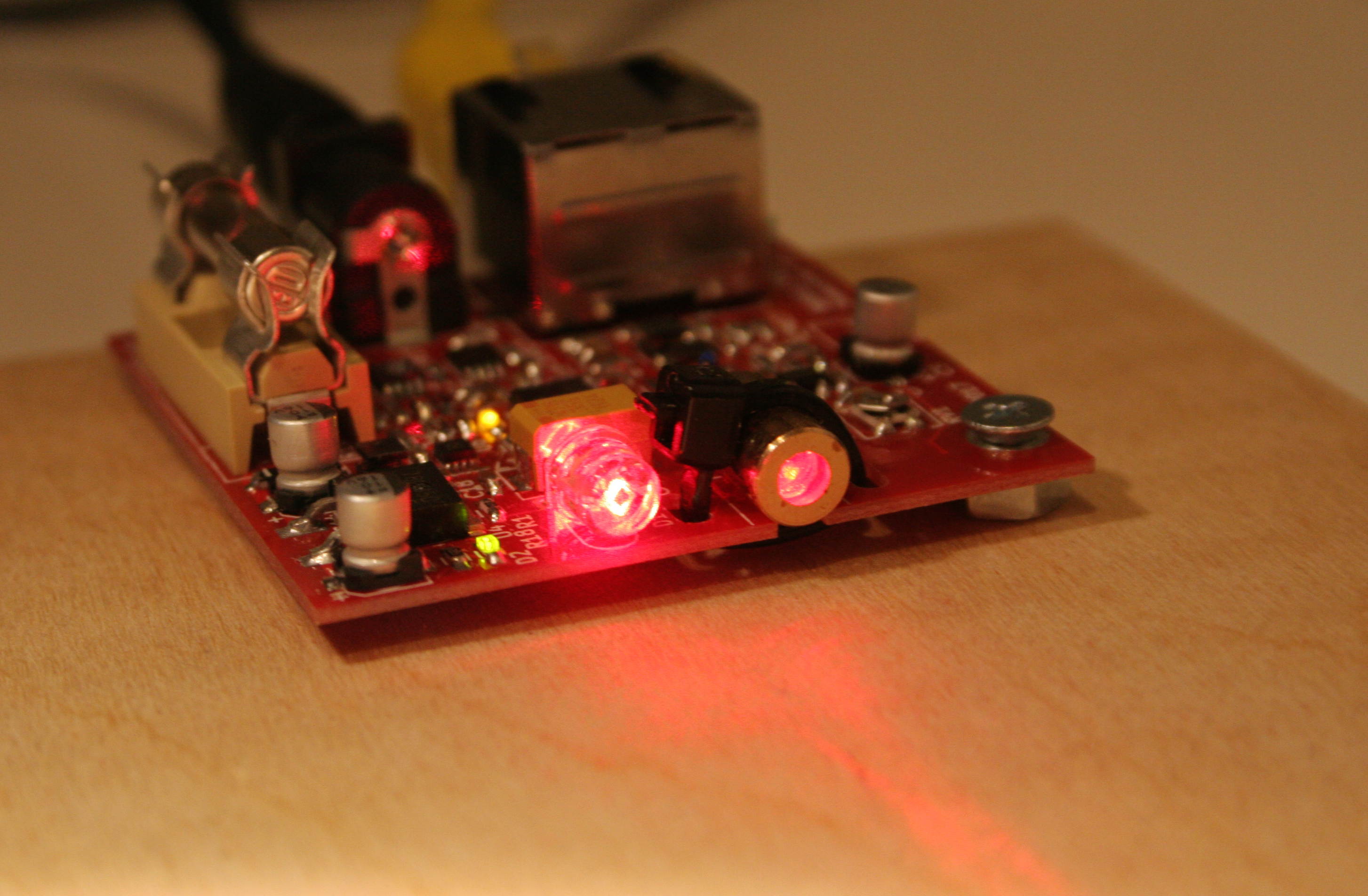
Because this sounds cool, I thought I could build something like that. Here’s the prototype:
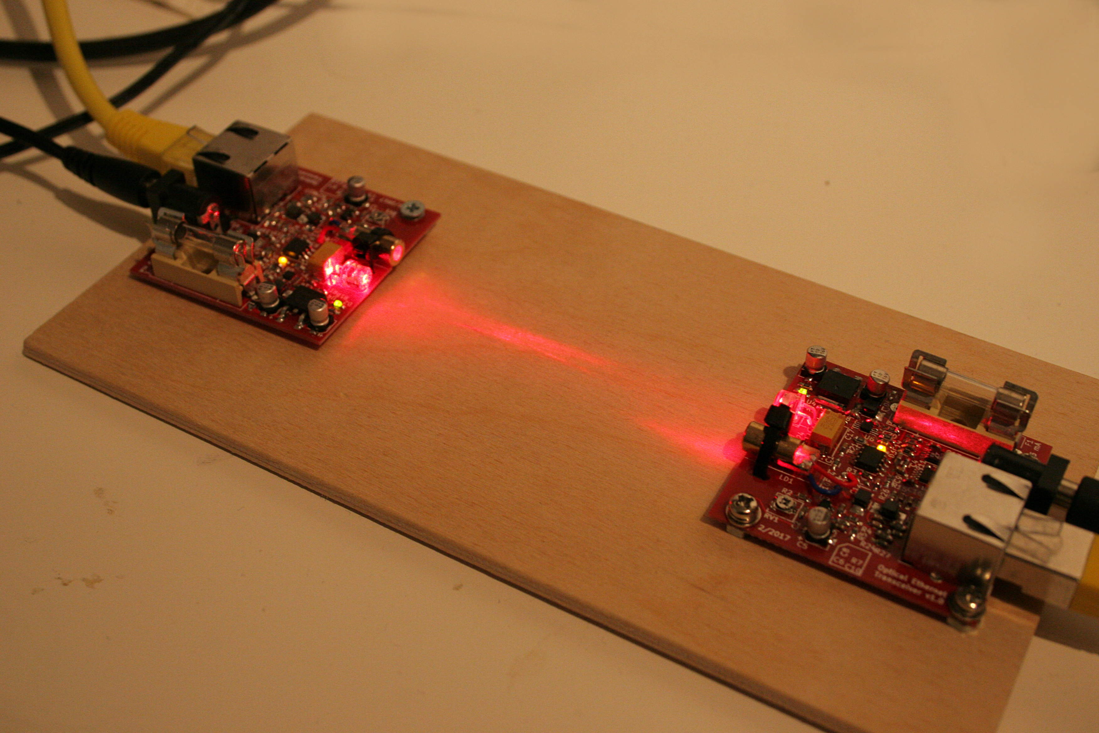
Laser ethernet transceiver prototype in operation
Concept
For simplicity, I decided to limit the scope to 10 MBit/s ethernet. This old standard is both conceptually as well as electrically (lower frequencies) simpler than the more modern 100 MBit/s or 1000 MBit/s standards. After a bit of research, I noticed that it’s not necessary for the transceiver to understand anything about ethernet; it’s sufficient to simply provide optical send and receive channels, and convert the electrical signal to optical intensity and back one-to-one.
The idea is now simply to build two identical boards with an ethernet RJ45 connector on the one side, and a send/receive optical transceiver on the other side. When pointed at each other, the boards mediate the ethernet signal from one RJ45 connector to the other.
Theory of operation
Each board consists of a transmit channel, a receive channel, and some meta components (power supply, fuse …).
Transmit channel
The task of the transmit channel is to take the electrical ethernet signal transmitted by computer A and convert it into an optical signal by varying the brightness of a laser diode. The schematic is shown below. The part with the operational amplifier is simpy a constant current source, which sets an “offset brightness” for the laser diode. The actual TX signal is then added to this offset brightness through AC-coupling (C23, C7 perform the coupling, R24, R6 set the optical amplitude, and L1 and L3 isolate the high-frequency signal from the DC offset current).
The bias current is selected such that in LOW state, the laser diode is still in laser mode (“glowing brightly”). With a modulation amplitude of about 4 mA and a laser threshold of about 12 mA for this type of diode, I set the bias current to 19 mA by tuning potentiometer RV1.
With this, we now have a laser diode changing its brightness in sync with the electrical signal of the ethernet twisted pair cable.
Schematic of transmit channel
Receive channel
The receive channel is slightly more complex. Its purpose is to detect the optical signal generated by its sister board, convert it back into an electrical signal, and drive that electrical signal into the receive (RX) cable pair of the conntected ethernet cable.
It starts with a transimpedance amplifier, which converts the photocurrent of a reverse-biased photodiode (SFH203P) into a power signal, with a gain of 1 kOhm.
The high bias voltage of the photodiode, about 35 V in practice, lowers the intrinsic photodiode capacitance and through that enables it to respond more quickly. This bias voltage is generated by an on-board DC booster (MIC2605).
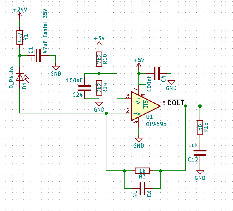
Schematic of receiver transimpedance amplifier
After this stage, the signal is still quite weak and noisy, as can be seen below:

Received signal after the transimpedance amplifier
To convert this into something which can be driven into the ethernet cable, a comparator (LT1713) is used. Conveniently, it already provides an inverted- and a non-inverted output, which makes it easy to drive a differential cable pair. Unfortunately, it does not support the high output current we need (5 V into 100 Ohms differential), which is why an additional dual operational amplifier is used as a buffer (MAX4392).
After the comparator, the signal looks much nicer:

Inverted output from the comparator.
The full schematic is available here.
Assembly
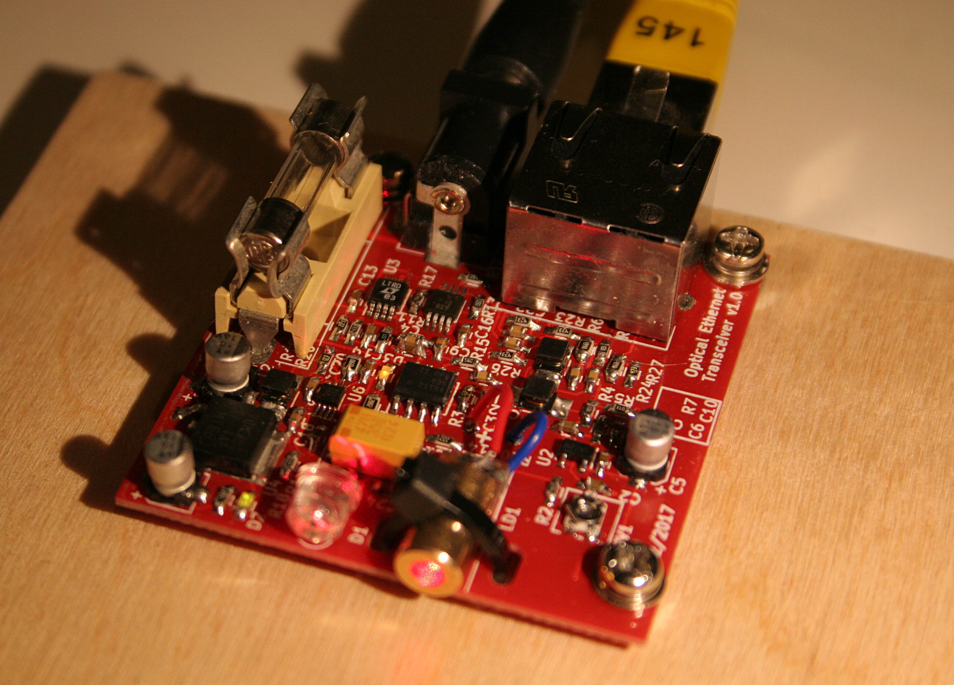
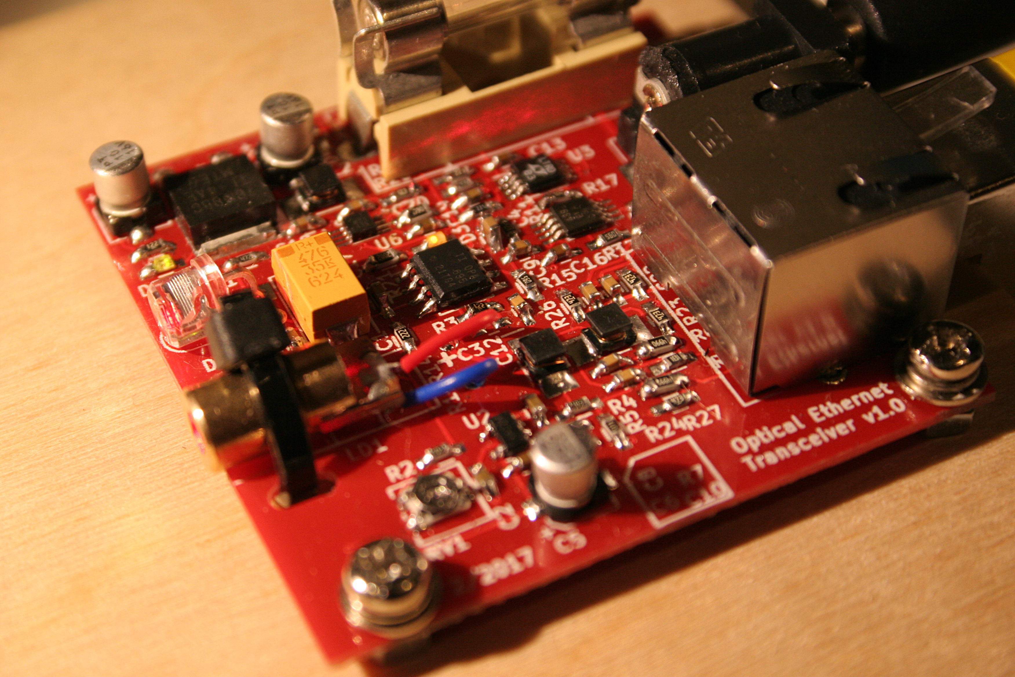
Armed with this schematic, I layouted a printed circuit board with SMD components in kicad, and sent it off for manufacturing. In addition to the transmit and receive channels and the DC booster, it contains a 5 V linear regulator, a fuse, and a 9 V DC input jack.
These are the manufactured boards (front and back):
Empty PCBs manufactured by Elecrow, top and bottom side. Size is 5cm x 5cm.
With soldering iron and a bit of help of the trusty chinese 858D+ hot air gun I assembled the first board step by step, testing the parts individually. Apart from one 200µm misplaced drill hole and confusing one “output latch” pin with “output enable” on U3 (both errors were easily worked around) everything went smoothly and this is the final board:
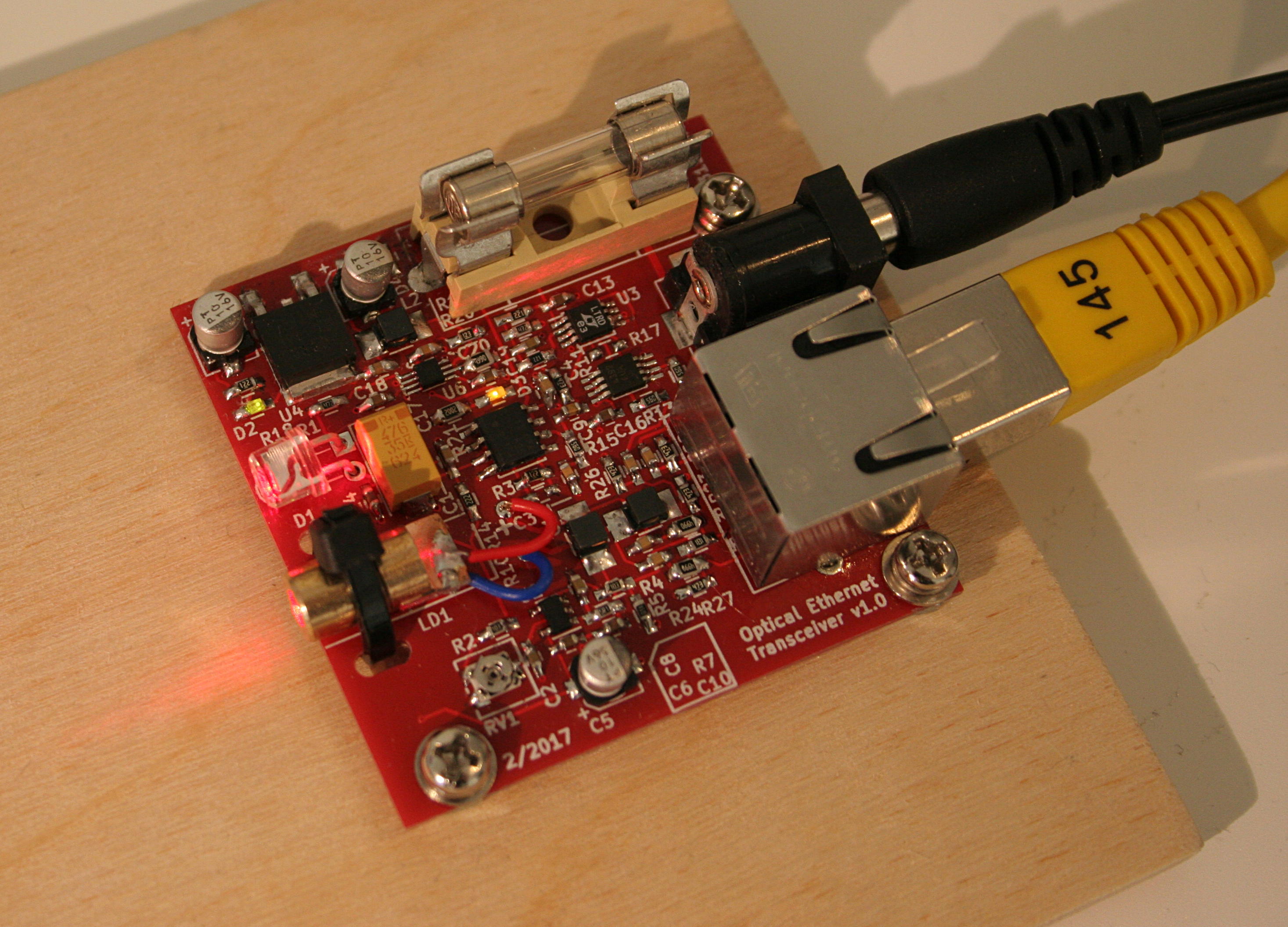
Final assembled board. The green LED indicates the presence of the 5 V supply, the yellow one is for the 35 V supply from the DC booster. The parts next to the big yellow tantalum cap are the laser diode (with red and blue wire) and the photodiode.
The laser diode is fixed with a simple cable tie. The screws have springs below them to allow for some tuning.
Insider question: if you look at the schematic, with C3 = 3.3 pF, U1 oscillates at something like 500 MHz. Why? C3 was supposed to highpass-filter the feedback loop and stabilize U1, not the opposite … with C3 not connected it works fine. Any insights welcome. Note that U1 is a current-feedback opamp, i.e. the inverting input is low-impedance. (Update: explanation here: http://www.analog.com/en/analog-dialogue/articles/compensating-current-feedback-amplifiers.html)
The next simple step after assemby of one board is to put a mirror in front of it and look if the transmitted signal is the same as the received one. And indeed, after some tuning, this worked and my notebook got confused by seeing itself in a mirror:
e1000e: eno1 NIC Link is Up 10 Mbps Full Duplex, Flow Control: Rx/Tx
IPv6: eno1: IPv6 duplicate address fe80::d6be:d9ff:fe85:330a detected!
This looks great! Thus I went on and built a second board.
Results
I mounted the two boards on a piece of wood and aligned the laser beams (not simple even for this small distance, unfortunately):
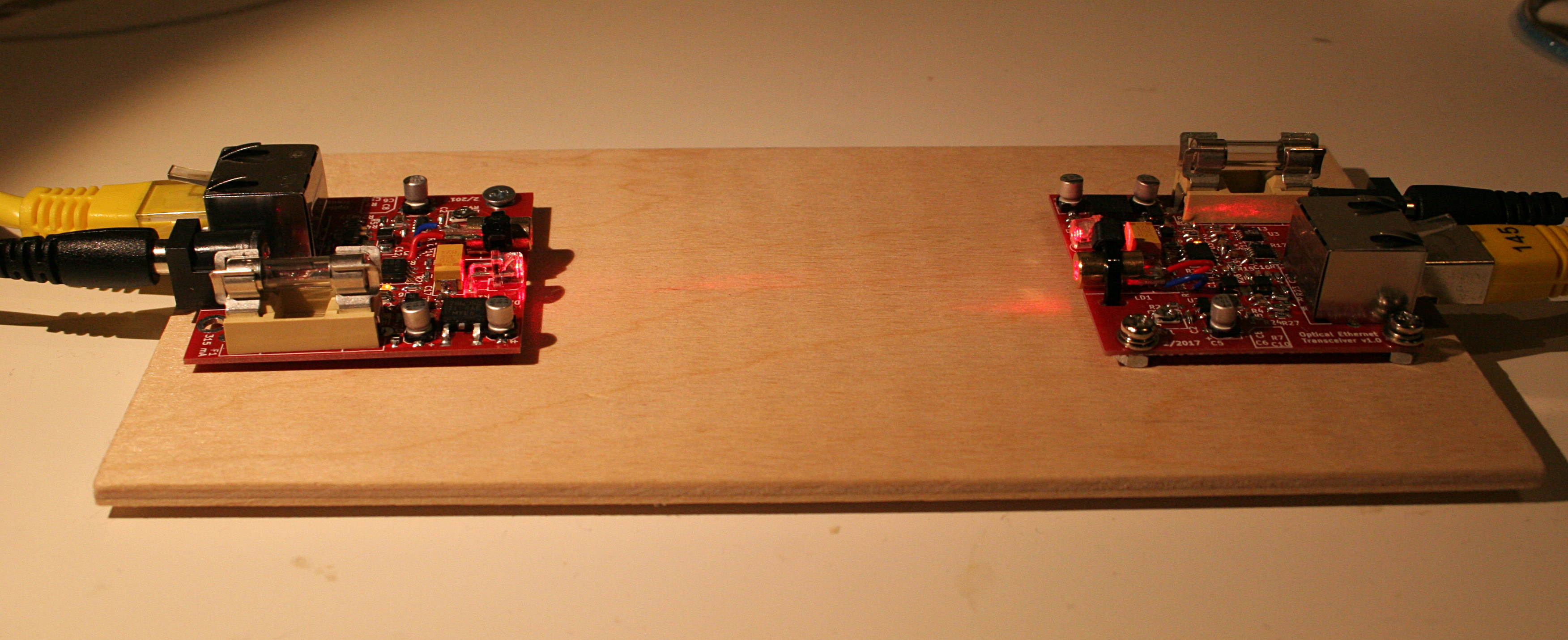
Test transmission section seen from the side. This is just about 10 cm of air between the boards (each board is 5 cm by 5 cm).
I booted up my Raspberry Pi as second computer and connected it with an Ethernet cable to one of the boards, and my notebook to the other one. And surely enough, they established a connection immediately:
e1000e: eno1 NIC Link is Up 10 Mbps Full Duplex, Flow Control: Rx/Tx
Fortunately this works even with auto-negotiation enabled (where the two computers decide on the data rate by themselves). This is not trivial, because both sides in this case think they support 100 MBit/s, but in practice only 10 MBit/s works. But for those two devices, after a few failed connection attempts with 100 Mbit/s, they switch to 10 MBit/s automatically (if this were not the case, it would be easy to force both devices to 10 Mbit/s mode manually).
Front view
I can also ping the Pi from my notebook:
» ping -i 0.025 192.168.1.52
PING 192.168.1.52 (192.168.1.52) 56(84) bytes of data.
64 bytes from 192.168.1.52: icmp_seq=1 ttl=64 time=0.843 ms
Transferring files over ssh works as well, with the expected data rate of about 1.1 MByte/s. If the lasers are aligned properly, there does not seem to be any packet loss, as tested by ping -f:
1799339 packets transmitted, 1799338 received, 0% packet loss, time 1465837ms
rtt min/avg/max/mdev = 0.597/0.753/11.748/0.049 ms, ipg/ewma 0.814/0.735 ms
Next step is to test this with a bit bigger distances between the boards.
Below are a few more pictures (click for proper quality and size).
Front view
Side view
- CentOS 6.8 image with Qt5.7, Python 3.5, LLVM 3.8
- Poor Man’s Optics: $50 Fourier Transform Spectrometer
Categories: Everything
Tags: electronics, laser
200 replies ›
Trackbacks
- Go Wireless with This DIY Laser Ethernet Link - worldnews
- any idea to what dp we re looking to sign? :tfc reddit - bankloginbook.com
This is really cool.
Great Work!
I have a question though.
Is there any blocker that makes you not use a pair of normal optical cables as a transfer medium ?
Well, the idea was explicitly to build a wireless link, so there’s that 😉
Otherwise in principle no; though you need a fiber coupling optics and an optical connector. That will make things expensive, larger in size, and reduce efficiency, at least for small distances, because the coupling efficiency into the fiber will be not very good.
Well done! This is a very interesting project.
I want to try it.
Can you sell the PCB, or maybe fully assembled boards?
Thanks! I don’t really want to get into selling things at this scale, it’s so complicated and somehow doesn’t seem worth it … I can certainly publish the design files though, or email them to you, so you can have some manufactured yourself (that costs something like $20 for 5 pieces), if you’re interested in doing that.
You would also have to buy the components though, and soldering is not entirely trivial (the DC booster for example is quite small).
I’m also not super happy with all of the design decisions; alignment is a bit difficult, the circuit is lacking ESD protection at its input, things like that, so before I would order new PCBs, I’d suggest a few changes.
Hi Sven,
You can Email me here: contact@ootsidebox.com
Ok! I’ll upload the design files later today and email you with a few comments.
Hi Sven,
Can you share to my email too: ddarlis@yahoo.com please?
Hi Denny, you can find the design files here: http://files.svenbrauch.de/laser-ethernet/
Have fun!
Sorry for late reply, thank you very much Sven
Hi sven,
Can you send the circuit too? I’m an undergraduate student working on my thesis and I would like to reproduce your work. Thank you very much!
What’s the maximum optical power output in normal operation and under fault conditions? How does that compare with eye safety regulations?
The last time I investigated laser diode characteristics, they had a very sharp V-vs-I-vs-Pout characteristics. That meant it was easy to overdrive them (until the facets disintegrated!) and they would emit dangerous amounts of light.
You’ve only got one pair of eyes, and they can be destroyed in an instant.
As people who work with lasers are repeatedly taught, “do not look into laser with *remaining* eye”.
Output power should be something like 5 mW CW, I don’t know exactly, I don’t have the necessary measurement equipment at home. The average electrical power going into the diode in normal operation is something like 7 mW though, so it can’t be much more. AFAIK 5 mW CW red is considered eye-safe even if you look directly into the beam (eyelid closure reflex will save you).
It’s certainly possible to hurt yourself with this diode though, if you do it sufficiently wrong. The trick with laser safety is not to look into the beam.
In my feeling, as soon as you have some orderly setup, the risk of hurting yourself even with a bright laser is quite small; you have a well-defined beam path, and you just don’t look into it, and all is fine. Caution is especially required during assembly and while experimenting.
So could the laser be replaced with an array of IR LEDs?
You can replace it by an IR laser diode, but not by plain IR LEDs, because you cannot collimate the output of a LED into a beam.
You can collimate LED outputs. It is a standard technique to increase both range and safety.
If the output isn’t symmetric then you may benefit from an aspheric lens.
Immediately after exiting the lens the collimated beam will be wider than the uncollimated beam before it enters the lens. More importantly, at the receiver the collimated beam will probably be narrower than the uncollimated beam, so more energy will be received.
Let me correct myself: you cannot losslessly collimate (incoherent) LED outputs. Incoherent LEDs (by that I mean non-lasing, non-superluminescent ones) have a large Etendue (see https://en.wikipedia.org/wiki/Etendue) which you cannot decrease by any means, and thus you cannot form a laser-like beam unless you discard most of the energy by using a slit.
Quite probably the beam quality of the laser diode could be improved as well by better optics, you’re right there.
I’m not sure what you mean by “losslessly”; the same energy exits a lens or reflector in the collimated beam as entered in the uncollimated beam.
Now, as I stated, the collimated beam is wider when it exits lens or reflector. If the beam area is larger than the receiver at that point then less power will indeed be received at that point.
However, if the receiver is some distance from the lens it may receive more power from the collimated beam than the uncollimated beam – and that’s what matters from the system point of view. It all depends on the simple geometry of beam width, divergence, and range.
And that’s why many real world professional commercial systems collimate LED outputs.
Do you have an example of a professional system wich collimates LED (non-laser, non-superluminescent) output to increase range? I think that is not possible and violates a fundamental law of thermodynamics, but I’m happy to change my opinion. You can decrease beam divergence for small distances by creating a convergent beam with a second beam waist, but that will make the beam diverge faster beyond that point in return. Maybe you can achieve some small improvement due to some secondary effect I overlooked, but a large improvement is not possible.
Yes, you can create a beam with a certain width, but the divergence of the beam will be related to the area of the light source you put in front of the lens. The amount of power propagating in the exactly parallel direction (in the differential sense) can only be increased by increasing the source area brightness density.
I’m afraid it is >35 years since I worked in the area, so any commercial equipment knowledge is out of date – and the equipment has probably never been described on the web! I do remember considerations similar to those you mention w.r.t. launching power into multi-mode optical fibres, but that’s rather different to free-space optics.
I’m sure there are rangefinders and free-space comms equipment with collimated outputs, but I’m not going to spend time looking for them.
Those use lasing or superluminescent diodes. If you could use simple broadband LEDs for range finders, people would love to do so (because most properties of lasers, such as temporal coherence, are actually undesirable for the application) — but it’s not possible. The exact same argument holds for fiber coupling.
Sorry I was thinking of an omni directional system but I had a brain fail and forgot that it would need to be duplex so the two sides would interfear with eachother.
So, you don’t know, and faults could cause >>5mW to be output. It could cause “life changing injuries”.
For starters, look at how little extra voltage/current is required to vastly increase the optical output. Now demonstrate what happens if there is a PSU glitch, or one component fails, or there’s an ESD into the worst possible node.
You really REALLY should look up and thoroughly understand the eyesafe limits. One point of reference is that in a classroom a laser even a 0.5mW laser is marked “don’t stare into it”.
Edit: removed part which I think is unsuitable in phrasing and content for this discussion. -Sven
I am not selling this device, nor am I using it in public space. I know about laser safety and I think I can realistically estimate the risk for myself.
This kind of laser is roughly in the 3R safety class. Lid closure reflex will protect you it, and while it’s certainly not safe to stare into it, accidentially inflicting serious harm to anyone with it is very unlikely. While it’s certainly bad to under-estimate dangers from laser radiation, you can also over-estimate it.
An ESD event will instantly destroy the diode, and a few-microsecond pulse of a higher intensity will not cause any harm because its total energy contents are not sufficient. The diode also dies very quickly if you power it with more than its design current, I tried that out inadvertently more than once ;p
Sven, this guy is obviously trolling or has no idea what he is talking about. Although he has added nothing to contribute to the conversation, I feel your responses to him are well thought out and I did learn a few things from them so I will give Tom credit on extracting some extra knowledge from you, albeit in a ridiculous way. I am very interested in this and would also be interested in looking at the board layout as well. I will post my gmail account and would love to learn more about this. Thanks
gorrell72@gmail.com
Hey Greg, I published the design files here: http://files.svenbrauch.de/laser-ethernet/
Have fun with them 🙂
License is CC-BY-SA-NC 4.0, ask me if you need something different.
I try to avoid mud fights with people on the internet, so I attempt to only reply to the factual statements and ignore / delete the rest … not sure what else to do.
Excellent project. I have been looking for a way to extend my network to another building, so this looks promising. What changes would be required to achieve 100MBit/sec?
Unless you are interested in tinkering with electronics just for the sake of it (like me), I’d recommend to buy a professional commercial product (i.e. not this) for practical use.
For 100 MBit/s I think you need quite some changes, I’m not even sure whether the concept of not having an extra MAC can be sensibly carried over to 100 MBit/s. I think if you want this with more than 10 MBit/s, it’s better to start from scratch.
Really excellent job, Sven!
This idea is something I had the intention to develop a few years ago during my Bachelor’s studies.
I also thought about using an USB to Ethernet board to make it “portable”, just for experiments and maybe ending with an USB to SFP “converter” (could be used for something like the Koruza project: http://www.koruza.net/).
Perhaps you have also come across other similar projects in the field of free space optics, for example this one regarding Li-Fi:
http://rishifranklin.blogspot.bg/2014/07/visible-light-communications.html
By the way, are there any spare boards left? 😉
Keep up the great work!
Kind regards,
Nikolay
Thanks! 🙂
Yes, I’ve seen a few other projects, mostly after I did this one already though.
I think the biggest issue with applying this in practice is the alignment, if you want it to be at least somewhat portable you need a concept on how to simplify that.
I have a few spare boards left (4 or something), I can send you 2 if you like. You need to buy a plethora of components though (costing about $30 per PCB), and you need some soldering equipment and experience to assemble it (the DC booster for example is in a 2mm x 2mm 8-pin QFN package with 0.5mm pin spacing and exposed pad).
Best,
Sven
Hi,
Very interesting project, would you mind to share the source off, or more details on the laser diode?
Best regards
Christian
Hi, thanks! Source files (kicad) are here: http://files.svenbrauch.de/laser-ethernet/
There are a few issues on the PCB still, esp. the drill holes of the ethernet connector are off a bit.
I don’t have any details on the laser diode either, I got them off ebay, and measured the characteristic curve myself. It’s specified for a maximum current of 25 mA apparently, is all I can say.
This is so cool! Question! If you used another laser ( blue laser led for example) and some wavelength filtering in the photodiode side maybe. You think full duplex could be achieved?
This is full duplex, by having two beams. By wavelength filtering, you could have the two beams use the same geometrical path, yes.
I remember that something similar was already explored, but in the sense of “Color-Division Multiplexing”.
A quick search revealed this:
https://www.extremetech.com/extreme/128207-1gbps-wireless-network-made-with-red-and-green-laser-pointers
Good luck!
Best regards,
Nikolay
Interesting link, thanks.
This is the absolutely standard approach though, any fiber network which uses a single fiber uses two different (typically IR) wavelengths. The idea of doing that probably dates back by 50 years or so. 🙂
Best,
Sven
Hi Sven,
great work. About the issue with C3 = 3.3 pF (U1 oscillates): Do you have used the equation(s) of the Analog Devices article linked by you? Bear also in mind that U1 and other parts are not ideal ones, e.g. the 47uF Tantal (C1) does not have 47uF at 10MHz anymore (actually I found a value of only about 3uF in a datasheet). Since the circuit is working well without C3 (doesn’t it?) I wouldn’t bother much about this.
Regards,
Stefan
Hi Stefan, yes, I used the equations, they come up with an ideal value for the capacitance which is extremely small (order of magnitude of the parasitics I’d say). And indeed, not putting any lumped capacitance makes it work …
The confusion just originated from the fact that thinking about a voltage-feedback opamp, putting a bigger capacitance makes it more stable. It bothered me that the exact opposite happened without a clear explanation why. It’s certainly fine like this now.
I’m aware about C1 — the frequency in question is more like 1 MHz though (dc booster switching frequency), and 3 µF is probably fine. I used a tantalum because every other option is even worse at 35 V.
Hey Sven,
On the KiCad schematic, there seems to be an issue with with how the program reads the individual integrated circuits. There is a question mark under each IC so that it cant properly register the U1,U2 etc.
Do you have an eagle cad file of this or can you repost a proper link?
Also do you know how to make fiduciary drill holes on the schematic?
Thanks,
Ben
Works fine here, which kicad version do you use to open it? Have a screenshot?
I don’t have eagle files, the board is designed with kicad and you cannot easily convert between the two.
What’s a fiduciary drill hole? Never heard that term.
Best,
Sven
I figured out the problem, there was something on my end.
Actually I think it is used for a machine to recognize the position. I was trying to add it to your PCB but it isnt so easy.
From the PCB manufacturer:
“Fiducials are used by the pick and place machine’s vision system to align the board. Here are ‘must-have’ requirements for fiducials. Fidicuals may be positioned underneath parts.
There should be 2 at opposing corners of the board
They should be metal pads, unmasked, at least .5 mm in dia with a 2x unmasked guard area surrounding them
They should be named FID1, FID2, .. FIDn in your BOM
Here are some ‘desirable’ characteristics of fiducials
Ideally, there should be 3, one in each corner, Two should share common Y values and Two should share common X values.
They need to be at least 10mm apart
If your boards are panelized, the fidicuals can be on the panel frame (but it is safer to put them on both so we can assemble your boards depanelized)
For more information on fiducials see http://www.ladyada.net/library/pcb/fiducials.html “
You seem to intend to get this manufactured professionally, i.e. with assembly … sorry, no experience with that. You can just add footprints to the PCB at will, though, in pcbnew; it should be easy to create a footprint which does what you need.
Hey Sven,
Why is it that I see the TX pins are 1 and 2 and RX are 3 and 6 respectively and they are reversed on the diagram?
http://pinouts.ru/visual/Ethernet10BaseT.jpg
Well, the TX of one end is the RX of the other, so you can’t really say one of them is TX or RX. The function is re-assigned randomly by the hardware for each connection, actually.
Sorry for the questions.
Shouldnt the tx always be the driver of the laser diode?
I am in Florida if you have any pcb left could I buy them off of you? I wanted to do this project to show laser communication to new students as a demo.
The network card selects which pair is TX and which is RX while establishing the connection these days. As far as I’m aware, it doesn’t matter how you wire it.
Hmm, I’m in Europe, and I won’t be where the leftover boards are for 4-5 weeks right now. Also they are all not fitted with components yet, so you’d need to do that anyways. It is probably both faster and cheaper if you just order new ones, sorry …
Thanks for the help though!
So you are able to solder the surface mounted chips by yourself on the PCB?
No problem, you’re welcome. Yes, I do that with an ordinary soldering iron and the occasional help of a $40 hot air gun (Atten 858D+), it’s not very difficult if you know how to do it. The footprints on this PCB are specifically designed to make it easily hand-solderable (esp. they have very long pads). Mind the errata “list” I posted above, the RJ45 footprint is still off by 100µm!
Last question, in the bill of materials that I have here I highlighted what I don’t know in red, can you resolve that by linking me with their Mouser link or Digikey?
https://drive.google.com/open?id=0B5fi0W66R_LSZHM2anF3OEs4R28
Also what exactly is the fuse and barrel jack connector?
C3 Do Not Connect: just leave this open.
C14, C15: any SMD 4×5.8 mm 10µF 16V electrolytic cap you can come up with
Fuse: standard 5×20 mm through-hole fuse holder
Barrel Jack: standard barrel jack connector — I think there’s only one common footprint which looks like this, e.g. http://uk.farnell.com/lumberg/neb-21-r/socket-low-voltage-2-1mm-4a/dp/1217037
Here’s some more:
– Ethernet connector: RJHSE-5380
– Tantalum cap: KEMET T495X476K035ATE230
I would advise to change the value of R2, and move R1 closer to the DC booster if possible to avoid short-circuits (I destroyed one of mine by shorting it to to the ground pad of U4 with a screwdriver accidentially …).
Could I use any SMD LED indicators? It looks like if I insert the right color, for the most part, they all have the same forward voltage I just need the right color? I am going to use HSMQ-C170’s for each respective color. https://www.digikey.com/product-detail/en/broadcom-limited/HSMQ-C170/516-3071-1-ND/4240315
Should that be ok?
As you say they are just indicators. You can leave them out or use different LEDs with different colors, the worst that can happen is that they are a little brighter. The one you suggest is 0805 though, I used 0603, yours will be a little large for the pads.
Can you email me your file \home\sven\Projekte\kicad_libs\newcomponents for this project at benastuart@gmail.com?
Hmm, why do you need that? Isn’t all the stuff in the cache?
Sorry, I can do in two weeks at the earliest 😉
Its okay, I mostly clarified it. The main reason was because of the pin styles for a component.
I’ve gone ahead and made way to order everything except for D4 and the type of fuse.
For D4 the model in the KiCad file says Capacitors_SMD:C_0603_HandSoldering except I thought it was a diode, maybe its not connected? If so if its an LED please clarify and if its a capacitor whats the value?
As you can see there are several fuses in slow or fast acting and different amperages with the same 5x20mm footprint. https://www.vellemanstore.com/en/fuses-73
Any idea as to which fuse?
I really appreciate all that you have done, and I believe this can be a really nice inspirational project for others to see.
I have LEDs with 0603 footprint, so I just use this to solder them on. It’s connected but it’s just an indicator LED, so if you leave it out it’ll be fine.
I used a 315 mA quick fuse. Something like a 500 mA quick or really anything in that direction will be just fine too.
D4’s an LED? It’s connected to 9V, though? And pointed the wrong way? And sorta where I’d expect an ESD diode to be.
hello sven my name is josh,
I was wondering how does power system work in this design?
thank you very much
You mean, how much electrical power does it use? Something like 200 mA I think, but I never actually checked.
hi sven,
I meant the power supply and fuse.
can you please explain what is theory behind the power supply?
thank you
josh
The theory is there’s an 7805 on the PCB and if you short it the fuse will blow. 😀
In addition there’s this little boost regulator which generates the HV (well, about 30 V) for the photodiode, but that isn’t really protectable by the fuse.
can you send me the pcb design please!
The design files are here: http://files.svenbrauch.de/laser-ethernet/
what software you used to open the pcb design File. please help me.
It’s called kicad and you can freely download it from the internet.
thank you
Todays technology (fiber optic) is basically fiber method. I am try to convert sfp transceiver to perform VLC through Led Bulb. Link 10 gb VLC
Very nice! I’m going to build this as a project for my telecom class in school (you will be duly credited of course)!
The DC booster (MIC2605) part looks pretty scary to me though, keeping in mind to make sure the thermal pad on it’s belly makes contact without shorting anything out. Any pointers on manually soldering it?
I soldered it like this: First, put a small amount of (leaded) solder on the pads, basically the smallest possible amount. Add some flux. Then with a pair of tweezers, put the part in place and hold it there. With the soldering iron, heat up the pads on both sides (that’s why they are so long in the footprint). Then with a hot air gun, heat it up again and tap it a little bit from above with the tweezers. You can probably do it with hot air right away as well, but I like to fix it first for parts this small. Good luck!
Do you plan to make your own layout or do you want to use this one? I still didn’t fix the positioning of the drill holes for the RJ45 plug, btw, they are off a bit 😉
Thanks for your reply! I’ll have to make adjustments so that it will be valid as a project. I’ll be adding an on-board 230 to 9V Coverter circuit to each of the two units as well as a case. I’m thinking it could be useful to make the laser diodes stand out on an adjustable limb (like on those USB keyboard lights).
I’ll of course be using kicad for the schematic and pcb! 🙂
Oh yes, if you do a new layout, definitely change how the laser diode is mounted, it’s not good like this. I think it would already help a lot if it was standing upright on the PCB, instead of on the side. In that case, with 3 adjustment screws and springs, you can actually align the beam properly (I would still try to use plate springs on the screws).
In that case you can also replace some of the parts, e.g. the OPA695 is completely over-dimensioned for this application (it has 1.7 GHz GBWP) and you should easily be able to replace it by something cheaper, I just used it because I still have it here from another project. Same goes for the MAX4390 in the constant current source.
Best of luck and I’d be really happy if you could post your results (layout and photos, maybe) here!
Hi Sven, this is a really cool project, I am just now getting familiar with electrical components such as op amps and the like. I was wondering if you could clarify something, I was looking at the schematic and it seems that when the data signal takes the value of a -1 that the potential difference across the first op amp (V+ – V_) increases? Would that not make the output also increase? And if so how does the laser diode respond, does it glow brighter when the data signal is +1 and even brighter when it is a -1?
Hey, which one do you mean by “first opamp”? But it’s quite possible it is inverting, yes … the signal is inverted several times. The transimpedance amplifier is inverting, for example.
The laser diode is biased to some “base brighthness” and then goes down from there for a -1 and up from there for a +1.
The MAX4390, I thought that a -1 would increase the brightness because it is increase the difference between the two inputs of the MAX4390?
Oh, that opamp is only a constant current source. It does not see any of the signal at its inputs, the signal is AC-blocked by L1 and L3.
Oh yeah that makes sense thank you for that. So one more question to help me understand does the laser diode dim because the -1 v signal decreases the voltage across the laser diode? Sorry for all the questions I’m trying to make logical sense of the circuit.
Yes, exactly, in one case the voltage increases, in the other case it decreases, and that’s why it gets brighter or less bright.
Hey Sven quick question, I made two of these at my house with the intent of connecting one side to the Internet. With each tranceiver I can get my laptop to think its connecting using a mirror so I know each one works. However when I plug one side to my router it won’t connect any thoughts?
Wow, awesome! Have any pictures of the finished boards? 😉
Well, one issue with this layout is that it only supports 10 MBit/s but the two sides don’t really know that. My devices try to connect at 100 MBit/s and then notice it doesn’t work, and go to 10 MBit/s automatically. Yours might not be capable of doing that. You should be able to set the speed manually to 10 MBit/s on both devices, then I’d think it should work.
Hey Sven, I’m doing a similar project and trying to create to create an SSH GUI over a client-server model. What I want to create is a better link communication and my priority is to check the packets transmitted and received among other statistics such as packets lost, speed and time required to send the data packets, just like you did. would it be possible for you to send you code file to this email: george_45a@hotmail.com? I’d really appreciate it. thanks and great job by the way .
Um, there’s no code. I just typed “ping -f 192.168.50.2” or so and then pressed Ctrl+C at some point. Read the ping manpage for more info. 😉
You could try to use WireShark for packet analysis. 🙂
yeah, that’s the thing, I have to create my own custom packet analyzer.
Hi,
A low noise 10mb optical transceiver can make you earn a lot of money in audiophile world.
On of the problem with digital auduo is the noise coming from the network. This has a juge impact on dac ships abd sound quality.
Some people put some linear supplies to thier ntwork equipments to reduce the noise and some others use optical bridge with optical/ethernet converter. Thise brudges perfeclty isolate the audio system from the betwork but the problem it that thise mefia converter are supposed to drive data on km abd the laser power and diods switch made them noisy by itselves (and most if them have switching supplies that ate a nightmare for audio).
Could you adapt you tranceiver fir such a need ?
(I would buy one at once)
Bernard
If i send you a close picture of the pcb of my media converter, would you be able to see if there is something i can do on it to reduce the laser power ?
Got this one on downstream side symupplied by lifepo4 3,3v batteries (for low noise and ac decoupling)
https://m.reichelt.com/fr/fr/Convertisseurs-de-m-dia/DELOCK-86443/3/index.html?ACTION=3&GROUPID=8135&ARTICLE=175547&OFFSET=16&
I took it because it has no inner switching regulator and i can decrease the power to 3v before it cuts.
Sven, this a fantastic project and one I’ve been looking for, for a long time. You’re a genius! My question is, if you shrank the distance between the two boards could you drive a 100Mbps? And let’s say you shrsnk the distance to 5 to 10 mm. Could you drive 1Gbs Ethernet?
Many thanks!
JW
Thanks! The answer is no, because both the driver and the receiver are too slow for that, because intensity wouldn’t actually increase if you decrease the distance, and most importantly because 100 MBit and 1 Gbit/s ethernet have different interfaces electrically that are not compatible with the approach used here.
What would be easily achieveable would be a faster receiver if you had more light, then you could just reduce the gain and it would automatically have a higher bandwidth.
Roger that, I understand. I guess my next question is could you design a 1gigabit method from scratch? Using whatever methodology would be required?
It’s certainly possible but for me would be quite a challenge, and for anyone it would be a major project. Pretty sure I would need more than one attempt to get it working.
Methodologically, the main difference from this approach here would be that you would almost certainly need to build this as something that actually understands ethernet, i.e. probably has its own MAC, and then uses some suitable modulation on the logical (not physical, like here) signal. On the receiving side you would need a demodulator which produces e.g. RGMII interface signals from the received optical signal, which are then fed into a GBit electrical phy. It would be massively more complex than this simple hack and also require lots of digital electronics.
Or, if you don’t want to do all the thinking yourself, what you would probably do in practice is using the SFP interface like for existing optical transceivers. Then you can probably use some off-the-shelf switch part which receives the 1 Gbit/s copper signal and translates it to the SFP interface, and only implement the SFP part yourself (ignoring the form factor for simplicity, probably).
Makes complete sense. Thank you for your patience and explaination.
Do you by chance have any schematics for a 1gbs copper to fiber (SFP) media converter. Your schematic we’re awesome. And I’d like to see what the faster componet schematic looks like.
No, sorry, don’t have anything at hand — maybe you can find something on the net 😉
help am trying to create a lifi internet receiver
i already have a transmitting 18 watts LED PANEL BULBS
sir
kindly help me with detailed steps on how to create an optotransciever on an empty copper substrate board
sir i was looking on the board to find the ADC on the receiver i want to know if an ADC was soldered to your board am asking cos am the verge of doing something like this but on a diffuse mode transceiver
waiting for your response
This project is not using an ADC, as you can see from the explanation above.
if the transmitter side is plugged to a dc for constantly charging electromagnetic field to ensue and the receiver side is connected to a desktop, laptop or phone will an internet connection be established?
my great friend this is a great project kindly send me the design files so I can try one out myself
my email is mitchoes@yahoo.com
great thanks brother
Links to the design files are in the comments above.
What a awesome work, beautiful professional like boards!
I’m currently making a project like this, for my graduation (Eletrical engineering), based on FSO comunitations sistems aplied on ethernet networks, than i saw your project! So, let me make some questions..
1) what is the purpose of the tantalum cap?
2) the r15 and c12 in the output of transimpedance amplifier is a kind of filter?
2) After the transimpedance amplifier, how do you conect the the imputs of the LT1713 comparator ? Seems like you put the signal in the 2 inputs trought R11, mixed with voltage reference part, im kind of confused..
Otherwise im planing to use LTC6268 for the transimpedance amp, since the datasheet shows a lot of information to this aplication.
Hi there, thanks for your interest and kind words!
1) The tantalum cap smooths the voltage produced by the boost converter. Since it is produced by a dynamic, high-frequency process, it will be very noisy, and that noise will couple into the signal across the photodiode, so we want to keep it as low as possible.
2) R15/C12 sets the output impedance of the amplifier to something low (50 Ohms). It is supposed to improve stability, but you can probably leave this out.
3) R9/R8 generate a threshold voltage. C11 stabilizes that. The threshold voltage is fed into the non-inverting input over R16. The signal is fed into the inverting input, after setting its offset voltage with R11. In addition, the threshold voltage is shifted a little bit into the current output state (so a bit towards high or a bit towards low) by connecting it to the output over the (large) resistor R17. This achieves a hysteresis effect, which prevents the comparator from immediately flipping back to its previous state after a state flip unless there is a significant change of the input signal. In other words, it makes the “low going high” and “high going low” thresholds slightly different, which improves noise immunity.
LTC6268 seems, like the OPA695 used here, at least one order of magnitude too big for this application (i.e. “too good” and thus too expensive). I just used the OPA695 because I had them lying around, I once bought 10 at a discount. 😀
Hope that helps and best of luck,
Sven
Tanks for the explanation, very intersting circuit, so r11 creates a dc offset to into the the imput alternating signa, right? In your case how much voltage you measure on the output signal of the transimpedance ? Im running some simulations here in LTspice, and got something like 50~100mv. In Analog devices website, i found a very intersting tool for for photodiode receivers, and you can export diret to LTSspice. Im my case im using sfh 213 photodiode.
http://www.analog.com/designtools/en/photodiode/
You can see it from the scope screenshot above, yes, about 50-100mV sounds accurate. The DC offset is required because we have no negative voltage supply, and we need to make sure the input to the comparator is always positive. And since we remove the DC offset beforehand with a DC block cap, we need to add it back in. This also makes the assembly somewhat robust to ambient light, which adds a DC offset.
Hello
I wanted to make something like this can u please send me pcb design file
Dude, you already asked me a year ago, and I sent you the link back then … see above …
Hi sven,
I’m a university student working on a design project and this design is very relevant to my project. I’d really like to learn more about your design, specifically about what limits it from 100 Mbps and from longer distances. Is there a way I can contact you?
Some of the other comments already have rather lengthy discussions about both these issues.
Feel free to contact me by email via mail at svenbrauch dot de.
You’ve mentioned that 100 Mbps and 1 Gbps have different ethernet interfaces than 10 Mbps, but from my research I think the 10 and 100 Mbps interfaces are the same (source: https://allpinouts.org/pinouts/connectors/networking/ethernet-10-100-base-t/). It seems to me that you could attain 100 Mbps using your exact design but with a faster laser diode, a higher power (for longer distances), a faster photodiode, and a faster driver circuit. Essentially, were you to have a higher budget and upgrade some of the parts, it would work. Are there major bottlenecks to these speeds I’m missing?
I don’t think your research is complete; as far as I know the major differences are a) 100BASE-TX is not DC-free and b) it has 3 signal levels, -1, 0 and +1 instead of just 2. Both goes against basic assumptions made in the design of this circuit.
Dear Sven,
Nice project, I would like to get information for the same project if possible please send the details at varungsit@gmail.com
I published all the design files already, see other comments 😉
Hi Sven, I’m amazed by your good work and I find it very useful.
I’m trying to do something similar to your project
I’d like to know which type of laser you used in the transmissor. Do you have the datasheet?
I want to try using a faster one in order to achieve higher speeds.
Thanks,
Luciano
Thanks! I don’t have a datasheet, it’s just those china laser modules you can buy from ebay or elsewhere.
The speed is not limited by the laser. This kind of circuit topology will only ever achieve 10 MBits/s, and if it were not for that, the laser driver opamp would be the factor limiting bandwidth.
Hi Sven,
I think this is very impressive and inspiring. I’m working on a project myself that has similar goals in mind and I’ll definitely draw from your smart design work. I would like to understand the process a little more in-depth. Specifically, would you mind breaking down more specifically how you chose the values of passive elements in your circuitry? Thanks!
Hi, can you maybe be more specific about which ones you mean? Explaining each choice of passive element values will fill pages 😉
The relevant ones in the receiving/sending path are mostly selected considering their characteristic impedance at the relevant frequencies (10 MHz).
Thank you for your reply!
Yes, so I’m mainly curious about C5,C6,C8,L1, and L3 as far as specific function. And then just in general, the values used on decoupling caps, like why that capacitance. Lastly, why is 10 Mhz the relevant frequency?
Thanks again!
C5, C6, C8 are kind of standard values and just serve to stabilize voltages which are meant to be constant. You could use different capacitance values here without changing much.
L1, L3 are selected such that they block the 10 MHz signal well enough from the DC offset current through the diode (generated by the opamp).
10 MHz is the relevant frequency since that is the clock speed of the 10 MBit/s link.
Looking at the datasheet from the MAX4390: https://datasheets.maximintegrated.com/en/ds/MAX4389-MAX4396.pdf
it says that the OA has a bandwidth of 85Mhz.
If we replace it with a higher bandwidth OA and adjust all the passive components to work at 100MHz, would it be possible to achieve 100mbps? What else should be changed?
(I’m a student doing my final year and I want to do a final project that could be quite similar to what you have achieved
I’m trying to explore what should I do to get >100mbps.
I have also asked in reddit. If you are interested, you can join to the discussion there: https://www.reddit.com/r/AskElectronics/comments/d3w151/laser_optical_ethernet_transceiver_through_open/ )
This whole circuit topology doesn’t scale to 100 MHz. I don’t know if you can reasonably build one in this style (i.e. without any microcontroller or re-modulator) for 100 MHz; it will definitely be more complex, since you need 3 states of the signal lines and also 2 channels IIRC.
I would like to know what color bands are used to connect to Rj45.
Hi! I’ve tried to connect two SFP devices without the optical fiber. I was trying to do something similar to what you did but I only got to achieve a 22 mm distance.
I’m not sure what could be the range limitating factor..
The optical power of the device is 1mW
The sensitivity of the receptor is -32dBm
Wavelegth: 1310nm
SFP: TFC-110s15 (https://www.trendnet.com/support/support-detail.asp?prod=375_TFC-1000MGA)
Transmitter Receiver: https://www.datasheets360.com/pdf/5569523322781363723
Photos of the experiment: https://imgur.com/gallery/Bz6w3Rl
Whtat’s the difference with your project? How did you achieve 10cm? More power?
Thanks!
Hi there, cool idea!
I think the problem with your setup is that the angle under which the light is coupled into the fiber is very steep. That means if you leave out the fiber, the light will spread in a cone with maybe 30° of angle, instead of a proper beam.
You can in principle add two lenses with the correct focal length for each device.
Is something similar happening in your circuit? That’s why you can only put them 10cm apart?
What could be added to your transceiver in order to increase the range?
No, my optical setup has a lens (it’s integrated into the diode) which forms it into an acceptable beam.
There is no real reason why you could only put them 10 cm apart, it was just sufficient to demonstrate the concept and easy to build. I’m pretty sure it would also work with a few meters distance, but if you actually try to do it, you will find it surprisingly hard to align the beams with sufficient accuracy. 😉
How do you know that the diode has a lens?
Do the lens help to counter the beam divergence?
I’d like to achieve 15 metres, would i need a diode with a small divergence?
Example:https://media.digikey.com/pdf/Data%20Sheets/US%20Lasers%20PDFs/M6505I.pdf
A diode mount (https://www.edmundoptics.com/f/laser-diode-mounts/12370/) is obligatory for the alignment at long distances?
Thank you so much for the all the answers!
Diodes without lens usually have very large divergence angles of several degrees in one direction, and several tens of degrees in the other. Your module seems to have a collimation optics built in, since it specifies a divergence angle of just 1.6 mrad, or 0.09 degrees. That would be a spot size of about 1.6 cm in 10 meters distance, computed by 10m * tan(0.00016 rad). Or just replace the tan function by its argument, it does nothing for arguments that small anyways: 0.00016 * 10 m = 1.6 cm.
From the area of this spot, the size of your detector and the total power of the module, you can compute how much power is available to your detector. If your calculations tells that this is not sufficient, you can use a collimation lens at the receiver side. Decreasing beam divergence below the 1.6 mrad specified for this module will be near impossible.
For alignment, you can buy something or build something yourself. In my experience, the mechanical assemblies from Thorlabs, Newport or similar are high-quality parts which are not that expensive if compared with building something of comparable quality yourself, so they might be a good choice. If you put something together yourself, that’s fine too, but you should aim to use screws for alignment and preferably build the mount of metal. Wood, plastic, paper, glue or tape are not materials that will make you happy in this kind of setup; they will always twist, deform or relax over time and screw up your alignment at the most un-opportune time.
Good luck!
Hey Sven. great work. I tried to replicate your work but I have ran into some problems.
1) In your actual pics of the PCB, R14 looks like a cap. Is that right?
2) Is R2 20k?
3) R17 is absent on the assembles pcb
4) You mentioned a misplaced 200um hole. Which hole you are talking about? And i believe on U3, LE should be connected to ground right?
I highly appreciate if you could reply.
thankyou
1. I don’t see exactly where you are looking but of C24, R14 one is a cap and one is a resistor. The pads are electrically the same, so it’s possible I swapped them on one of the boards (without effect).
2. I don’t have the board at hand at the moment, I buried it somewhere, so not 100% sure. 20k sounds ok though, change it for something smaller or bigger if you cannot get the desired base current by tuning RV1.
3. No, I think it was just removed for the first photo because I was figuring out the LE issue.
4. One of the mechanical drills of the ethernet jack. Yes, LE should be Gnd.
Hey, thanks for a prompt reply.
I have soldered R14 and R17.
Without R17, ping works, but a lot of packet loss, 50~75%.
With R17 soldered, PCs wont connect to ethernet at all.
Is there anything that i am missing?
and BTW, i needed crossed ethernet cables for it to work.
Ah cool, you built it? Nice! As said, I think there are far better component choices than mine, they were based on stuff I had lying around.
Check the signal at Pin 6 of U1 with an oscilloscope. Does it have enough amplitude? Try increasing R3, e.g. to 12k or even 47k. Does that help?
You can also decrease R6 and R24 (both by the same amount), to e.g. 100R, or increase or remove R22. This increases the amplitude of the modulation. IIRC I did that as well, now that I’m talking about it …
R17 adds hysteresis to the comparator, it seems like it is too large for the signal amplitude you detect. That is not the root cause of your issues, though, I think the hysteresis intoduced by R17=100k is sensible.
Crossover cables might be needed for very old devices, but modern devices typically do the switching internally automatically ..
Hi Sven, I got the same problem with Sam1 when I tried to build the pcb board based on your Kicad design. The PC didn’t connect to the board, so I changed the value of R24,R6, and even R22. And the problem still exist. The voltage comes from pin 6 of U1 is 3.5V, and I noticed the voltage from the DC booster Mic2605 isn’t 30V, it’s only 9V. Do you have any ideas how to fix it? Much appreciated your input. Thanks
Hi, the voltage from the booster isn’t very important, I think you could even leave it out. What do you mean by “PC didn’t connect to the board”? It will only connect to another PC with another board. Probably that was just confusing phrasing by you. 😉
For debugging, do you have an oscilloscope available? Try measuring the output signal at the laser diode, and the input signal directly before the comparator. What do they look like?
Hi Sven, thanks for your response. I meant the PCs don’t connect to the Ethernet at all. And yes, I do have the oscilloscope. Can I have your email, so I can send pics of the output and input signal from my boards? I’m already out of ideas to fix it. Thanks again for your input.
Hi, I sent you an email to the address you made the comment with, let’s continue there then 😉
Sven,
Amazing work!
I’m in a group and we are studying your device and are having a blast. However, like Brian, we’ve built the board but are encountering trouble with our computer detecting that the board has been connected. I see that you used E1000E to emulate a network adapter. Is this something that is required in order for our computer/Pi to recognize the board?
Any assistance would be greatly appreciated.
Hi, a computer cannot detect that this board has been connected, it electrically acts like a piece of cable. You need two boards and two computers if they are supposed to detect each other.
I didn’t emulate anything, I think that’s just the driver for my network adapter 😉 The only thing which might be necessary for your network adapter is to set it to 10 MBit/s mode automatically. Not all devices I tried managed to notice that even though their peer advertises to support 100 MBit/s mode, the connection isn’t actually capable of this.
Hi Sven,
Sorry to bother you again, I’m trying to understand everything before I start building the transceiver.
As I told you before, my main concern is achieving a minimum distance of 10metres.
You said that aligning the the devices would be a more difficult task as the distance increases.
I was thinking of another alternative to circumvent the problem, I want to increase the optical power.
What if I use a Laser diode of a ~80mA or more?
Moving the potenciometer RV1 I could increase the bias current and then I could use a differential amplifier (https://i.imgur.com/UZkgHap.png) to increase the signal voltage.(would this increase the signal current?)
With a stronger optical power at the transmitter, I wouldn’t have to worry so much about perfect alignment at ~10metres or more
Thanks!
I don’t think the alignment requirements decrease in a significant way if you increase optical power. You have a 2 cm red dot and you need to align it such that it hits the photodiode of the other part, and that dot being ten times as bright doesn’t make the job easier 😉
Instead of increasing power (and making the device non-eye-safe), I would first start with putting a cheap lens in front of the receiver to collect all of the beam power, if I wanted to increase range. That could also simplify alignment, because you might be able to shift the lens to do the fine adjustment.
I thought I could build something like that
Is it possible to establish an internet connection with this thing? Like e.g. you’ll plug one transceiver in your home Wi-Fi router’s ethernet port, then the other transceiver to a computer, will that work?
Yes it should, the only hurdle could be that you have to convince your router to use 10 MBit/s mode even though the connection advertises 100 MBit/s. Some devices are smart enough to automatically downgrade to 10 MBit/s mode if 100 doesn’t work, others are not. Some devices can be configured to 10 Mbit/s only. If neither works for your device, it might be a problem, but otherwise it’ll be fine.
Oh nice. I’m going to build this thing.
The only problem I’m facing right now is where I could buy the components that my local electronics store don’t have. I’m currently looking for alternative components, especially op-amps, comparators, and that boost regulator you used, because I really struggle to find the exact component.
Do you have any alternative recommendations on the components that I can use to substitute? It would be the best if I can use commonly available components, like an LMxxx series op amps.
Hi! Actually, because this project sees continued public interest, I recently started creating a redesigned version of it which uses both less and also more commonly available components. It’s not quite completed yet, unfortunately. I’m also currently wondering if I can sell kits for that version (i.e. you get 2 PCBs plus most required components for $100 or so), but unfortunately German regulatories around selling things like that are completely insane, so it might not be worth the trouble.
If you want to start your own modified design,
– the boost regulator doesn’t really matter much, you can probably omit it altogether and just connect that net to ground or VCC instead,
– the TIA opamp is the most critical, and requires careful selection so it is fast enough — I recommend an LTSpice simulation before you build anything,
– the output opamps and the current source are also a bit troublesome in that they need to be able to supply > 20mA of continous current over their full output swing.
Best of luck!
Are you planning to release a redesigned version publicly? That would be great!
Well, for op-amp selection, if that’s the case, I’ll probably order some parts online instead.
For the other components, (resistors, capacitors, inductors, etc.) can I use regular THT components instead of SMDs? Is there anything to consider or will it have an effect to the circuit?
I would advise against doing that. If you like, you can design your circuit with larger SMD components (e.g. 0805 or even 1206). You will quickly notice that, once you did it a few times, SMD resistors are actually way easier to handle than THT. For example, they can be desoldered with zero effort by just placing a solder blob on them and pulling it away.
Apart from that, this circuit is not exactly DC, it contains frequencies up to 50 MHz or so. Especially around the input transimpedance amplifier, I place a ~1.5 pF or so compensation cap. I can imagine that with careless circuit design (“everything becomes very large”) you will have parasitics that make it just not work.
I have not yet decided what exactly I do with my reworked version, but the schematics at least will most likely be made public.
I will stay tuned for that reworked version.
I’m willingly love to work with SMD components though, but sadly, I don’t have the right tools for that. I only have a cheap chinese soldering iron that doesn’t even have temperature control. I can’t even find a replacement tip for it.
I looked for parts online, only to find out that I cannot afford most of the major components. That’s why I’m staying tune for your reworked version, hoping that the components you’ll be using are cheaper, since most of the time, commonly available components tend to be less expensive (that’s the case in my country, poor philippines). And I’m still a student that’s why I can’t afford it.
That’s the only hope for me to be able to do this for my school project.
Yeah, this version is not cost-optimized at all, it is optimized for “easy to design” and “components I had left over from previous projects”.
this is so cool
i will also stay tune for your redesign dude
when you will release it? i cant wait to build this thing
Next few weeks probably, I’m still clarifying whether I can sell it as a kit (i.e. you get components + PCB and assemble it yourself). Schematic will be available on the blog either way, though.
hello sven, i have questions
1. can i just use 24v power supply or a boost converter module in replacement for the mic2605?
2. is it really required to use smd components than using big regular components? smd components are not suitable in my case since i’m planning to make this on a prototyping board instead of getting my pcbs manufactured. i want to replace smd resistors, inductors, and capacitors with bigger ones. (in case of some components that doesn’t have regular version, i’m planning to use breakout board for them)
1. Yes, or simply connect the net to 9V, 5V or even ground, should work as well.
2. I’d argue that “regular” components are SMD since at least 15 years 😉 but trolling aside, in principle yes, but you have to watch out for high-frequency issues. If your comparator output couples into the TIA input, you will easily get a non-working circuit. I don’t know how hard it is to mitigate these issues with THT components for this particular circuit.
Hi Sven,
Thanks so much for this great work! I built two boards following your schematic but I am kind of stuck. Here are the steps I followed:
1. I built two boards, changed R3 to 47k and R6, R24 to 100R.
2. Each board is connected to a Raspberry Pi and I was able to perform the loopback test as you described with each board.
3. I then tried to set up a connection between the two Raspberry Pi, each connected to one board. When forcing the Pis to 10Mbps, the Pis do connect to each other.
The issue is that even if the OS shows that there is an ethernet connection, I cannot ping one Pi from the other.
Do you have any idea what could be the issue? Thanks again!
Hi!
First, did you try the exact same software setup with a network cable? Does it work then? Just to make sure it’s no software issue (misconfigured address, etc).
If that works, then the most likely reason is that the signal is good enough to establish the link, but large amounts of data don’t get transmitted correctly. Do you have an oscilloscope? Look at the signal before and after the comparator, do e.g. the low and high pulses have approximately equal length?
Greetings!
Thanks for your quick reply!
Yes, the connection works with a network cable in the same exact configuration.
I can’t get a good read of the ethernet signal when connected to the Raspberry Pis. That might be due to my oscilloscope that is quite old.
I can generate a 10MHz sine wave with Vpp=2.5V with a function generator. When I send this signal on the Tx of one the board, I can read the signal at the input of the comparator (before C9) on the other board and I measure a 10MHz square wave with Vpp=3.8V at its Rx.
Does that sound right? I am thinking to decrease R17 to soften the hysteresis.
Thanks so much for your help!
Ok, that you can’t get a good read of the signal is IMO a good sign, you will not be able to do that with an analog scope, since the digital data transmission isn’t periodic. This means data is actually being transmitted.
I think what you want to do is judge the quality of the near-rectangle signal that goes into the comparator at the receiving side. Can you set your function generator to generate a 10 MHz square instead, and look at that? Does it look somewhat even? Compare to http://blog.svenbrauch.de/wp-content/uploads/2017/02/DS2_QuickPrint15.png, that’s not ideal but at least not completely unlike what it should be like. Especially look if the rising and falling flanks have the same rise and fall time.
Unfortunately, I also have an old function generator that can barely make 10MHz signal and 10MHz square signals actually look like sine signals haha.
One thing puzzles me though: I measure a signal alternating -/+5V and 0V at LT1713 outputs and then a signal alternating -/+4V and 0V at Rx-/Rx+. That means the circuit output a differential signal with -/+4V (or Vpp=8V) while 10Base-T signal works with -/+2.5V (Vpp=5V), right?
Hi,
IIRC 10BASE-T even uses only +1/-1V according to the specification. But as you can see, the other transceiver also outputs more than that. If you are worried about this, you can increase the series resistors at the output, but in my (limited) experience, the receiver doesn’t care. The signaling of 10BASE-T is usually extremely robust, with transformers at each wire pair etc.
Also consider that cable lengths up to 100 m are supported (don’t know if by this transceiver, but by conformat ones), and there will be quite some voltage drop accross that distance.
I’m 95% sure this is not your problem.
All connection issues I had so far were because the signal shape wasn’t good. One thing that can easily happen is that the negative current drops the diode below the lasing current, and then the rise time is very slow. This can be mitigated by increasing the bias current, or decreasing the modulation current. But unfortunately, without a digital scope this is just guesswork. If you have the chance, I really recommend buying one, it’s a great learning experience also not that expensive any more these days. It will be well worth the investment just because of the things you learn.
Hi Sven,
I figured out a way to send a 10Mhz square in the circuit and proceeded with measurements as you suggested.
The signal that goes into the comparator at the receiving side looks like yours. Fall and rise times look the same as well.
After the comparator (LT1713), the low and high pulse do not have equal length anymore. You were spot on! Not sure how to fix that though… Any insight would be very much appreciated!
Hi,
how different are the lengths? You can see in my screenshot in the post that also in my version it’s not perfect (but still works). But if it’s too far off it will not work any more.
I’m honestly not sure where the effect comes from. Maybe the hysteresis is too big? It’s really hard to tell from afar.
Greetings!
Hi Sven,
I fixed a few solders and decreased the hysteresis and the outputs of the LT1713 now look great – very similar to your post. However, I still can’t get a connection.
I checked the Rx of the boards and the signal is not as good. There is a break of slope in the rising edge that modifies the square to a trapezoid waveform.
Do you have pictures of the output of the MAX4392 or of the board (Rx+Rx-) by any chance?
Thanks again!
Sorry, I don’t have a picture at hand, but if you upload one we can look at yours 😉 That the signal quality degrades a bit is to be expected and shouldn’t be a problem.
Are you sure btw that you set both of your devices to 10M mode? Not all devices automatically notice that 100M doesn’t work.
Thanks! Here is a picture illustrating my current problem. LT1713 output is in blue and MAX4392 output is in yellow. https://drive.google.com/file/d/1QwmzzLUxLtzNqWSGShBwSvdumcueFwPO/view?usp=sharing
Yes I do force both devices to 10Mbps and they do connect but ping doesn’t work. So frustrating!
That almost looks like it’s driving against something else in the first dip, don’t you think? Like, there are two phases, first with like 1V and then it goes to like 4V. It looks a bit like the 1V one is caused by something else driving this line to 0V during that time.
Maybe there’s a short somewhere? Does this look identical on both your boards?
Hi Sven, I have built the boards but I’m having trouble finding the problems.
We are using a wave generator for the signal source. And an oscilloscope for testing.
https://i.imgur.com/SpVeehm.jpg
First test: using only one board
Wave generator connected to RJ45 pin 3 and 6
https://i.imgur.com/16KSL4L.jpg
Freq: 5MHZ (max freq by wage gen)
Waveform: Square
Amplitude: 2.5V
Offset: 0V
Transmitter:
oscilloscope probe in laser LD1
https://i.imgur.com/ZQwGJdv.png
We can see AC of 5mhz with a 4V CC. Looks ok
Receiver:
oscilloscope probe in R15 and ground
Looks like a CC when the SFH203 has no direct light. The CC amplitude “moves” when direct laser light impacts SFH203.
Receiver:
oscilloscope probe in R1
5V with noise. Voltage increases to 6V when direct laser light impacts (distance: 1cm or less)
https://i.imgur.com/kGKMZqm.png
We have tried connecting the oscilloscope probe to the pins 1,2 of the RJ45 but we have no signal.
As far as we know. the transmitter looks like it’s working ok.
Is the SFH203 not working?
Laser: VLM-635/650 (https://www.digikey.com/en/datasheets/quartoninc/quarton-inc-vlm-635-650-03-lpa-lpt)
Hi, your laser data sheet says they have an “automatic power control” circuit built-in. This won’t work. It most likely filters out the modulation current we apply. You need a naked laser diode, not a laser module with an integrated driver circuit, since *we* are building the driver ciruit. 😉
Try these, they are surely available from an ebay seller in your country as well: https://www.ebay.com/itm/353187914842?hash=item523ba3e45a:g:uSAAAOSwXmRfUgIK&var=622388947162
Hi Sven,
I have a question regarding your comparator implementation. Your 470Kohm R17 and 220ohm R16 values give an approximate hysteresis of only a couple mV. I found the curious as on a 100mV signal as you have on your scope readings, this should not provide much of an effect as the signal noise is likely higher than this. I’m curious if you had any issue with such small hysteresis value and why you did not utilize a larger amount of hysteresis.
I have tried to implement this circuit have it mostly working. I’m having issues getting the comparator to behave correctly. The circuit works as expected when using a function generator however when it was not working as expected when an actual ethernet cable was tried. I’m using a laptop and a pi, both fixed to 10BaseT full-duplex. I believe I found the reason why. With a constant alternating source the comparator works as expected as shown here with the signal hitting the thresholds https://imgur.com/kIIjCdq
However, during the auto-negotiation phase of ethernet, there’s just the 100nS NLP and FLP pulses which are quite spread apart. This makes the signal mostly DC and the signal shifts up to the Vbias(bias voltage made by R8 and R9) during these long(>50uS) times between pulses. When a pulse finally does occur the signal has shifted upwards by 1/2 the signal amplitude making the falling edge miss the lower comparator threshold. https://imgur.com/ClaXzYH
I’m surprised to see this was not an issue you or any other commenters have faced as it seems inherent to the design. Once the negotiation phase is finished everything should work as expected, I’m curious if you had ever run into this “shifting signal bias voltage” issue and how you got passed the ethernet negotiation phase with this circuit implementation.
Thanks,
Mike
Hi Mike,
I don’t think the hysteresis is much of a problem either way. The signal edges are quite fast, and the comparator is not that much faster than the edges anyways — so even without any hysteresis, I would expect the circuit to behave correctly. I mean, you will only have a problem if the comparator can toggle back and forth *during* the time the input edge is less than the rms noise away from the trip threshold. This part by far isn’t fast enough for that, I think.
Your other comment in contrast is a quite severe problem with my design, you are completely correct. I also noticed this a while after writing this article. I’m still not sure why my circuit works nevertheless; I suspect some ringing or noise being enough to trip at the autoneg pulses, and after one of them comes through everything is fine, as you said.
I designed (and built) a different version which I think does not suffer from this problem. It also works with components with about a tenth of the price: https://i.imgur.com/bMA3eI1.png
However, I’m not happy with its reliability and couldn’t really figure out what is wrong so far, otherwise I would already have updated the article. 😉
I talked to most of the other commenters, but my impression was that few people got far enough to have the circuit built electrially as shown in the schematic, so they didn’t arrive at this level of problems.
Thanks for your message!
Sven
hi seven maybe could you resolve with a opamp with higest Slowrate from your response in a opamp in comparator mode with histeresis or inverter gate like a HC132.
Hi Sven,
I’ve been reading through your article on the optical ethernet-transceiver, and I found it very interesting, as I have some interest in this field of electronics.
In your last blog dated August 2021, you stated that you were in the process of updating your original design to accommodate some design changes and to reduced costs – So, since it’s been awhile since your last blog, have you updated the design, and if so, would it be possible for you to send me details of the circuit changes?
Thanks,
Phil
Hi, I have a new prototype of the circuit but you can read here in the comments that the current design has a bit of a flaw w.r.t. detecting the link pulses, which are not transmitted in a balanced encoding. Whether that works correctly or not is basically a matter of luck. While the new design had attempted to address this flaw, it still doesn’t work as reliably as it should, and I never got around to figuring out why. So sorry, the new design isn’t really done, and there are currently no concrete plans on changing that. (I had originally hoped that I could sell PCBs + components of the new design as a small DIY kit since I felt a lot of people would like that, but it turns out legislation around this is way too complicated to make it worth the hassle, so this effort eventually died down and with it the finalization of the technical side. To clarify, I would still have published the schematics and everything, so it’s not about money — providing the kits was just my motivator for the update and it’s kind of gone now)
I have uploaded the current version of the files to http://files.svenbrauch.de/laser-ethernet/, in case you are interested in continuing from that state. IIRC at least one footprint size was wrong on that PCB, but maybe that only affected my order.
This design is kind of cost-optimized and also tries to keep the amount of different components low, which is in stark contrast to the first one.
Hi Sven, I’am looking at the new design and I have some doubts about the purpose of the new components.
Could you make a small explanation of what changed?
For example: what are the Diodes 824001 doing?
Why is the Photodiode in Direct (and no Reverse as before, also no 24V)
Did u manage to make a transmission between two PCs with the new design?
Thanks,
Luciano
Hi, phew, not sure if I recall everything correctly. I’ll try.
The TVS diodes are for ESD and voltage offset protection. They ensure that e.g. the input from J1 pins 3 and 6 is always somewhere between our Ground and our +5V. Ideally, you’d have a transformer there in front I think, but just this is better than nothing.
The photodiode polarity… doesn’t really matter in this configuration with no reverse bias I think? It just flips the output signal if you flip it. The previous configuration also used a current-feebdack opamp, not the case any more. But here I could misremember.
The reverse bias is gone because it’s complicated and expensive (component-cost wise) to generate the +24V and it’s not really necessary. It reduces photodiode capacitance but that is already quite low for this photodiode; the bandwidth is mostly limited by the OpAmp IIRC. And it’s fast enough anyways, this I simulated in advance with ltspice and it is also true in practice.
The design did work under the right conditions, but it still suffers stability issues (which is why I didn’t want to publish it). I’m not sure why, it only establishes a connection with a lot of light even though from the signals I’d think it should work with much less. It’s probably related to some screwup with the DC offset of the output signal — it’s hard to get this right for both packet traffic and the link pulses used for establishing the link. Let me know if you have any ideas.
Hi Sven,
I am looking at the new-beta-unfinished-design and I have a question regarding D4. Is it currently placed in between the barrel jack and the Linear Voltage Regulator. Is that an error in the design?
If it isn’t, do you have any recommendations on what component it should be? Maybe any LED with a certain voltage rating?
Thank you!
TC
Hi, this diode is for reverse polarity protection. Any SMD 1206 package Schottky diode will do. Or any diode, really. Or a piece of wire, if you don’t plan to supply reversed polarity voltage 🙂
My BOM says the part number I used is SD1206S020S1R0.
What was the new beta version supposed to do, compared to the old one?
H, is great adapter have you think to modulate the TX signel?
I want to buy it where can I buy it could you please sell it on amazon
You mention the tantalum cap you used was KEMET T495X476K035ATE230 – how particular is that choice? I notice that there are far more T495X476K035AT in stock (at jlcpcb) but their specs are slightly different.
Oops, edit: far more T491X476K035AT in stock
I’m adding JLCPCB component IDs to the KiCAD project so you can just export it with JLCPCB’s plugin, import it to JLCPCB, and get some assembled.
https://github.com/Erhannis/LaserEthernet
Notes and questions:
1. They didn’t have any 15k pots in stock, so I used a 20k pot; I figured that was alright, yeah?
2. Likewise I swapped out the MAX4390 and used AD8051 instead; they look equivalent.
3. LM78M05CT isn’t actually an SMD component, looks like? But it’s a 5V regulator, so I used a CJ78M05 which I think should be the same.
4. JLCPCB lists like, dozens of barrel jack connectors (but calls them specifically “shrouded power receptacles” fyi), but I think this one may be close enough? https://jlcpcb.com/partdetail/ShouHan-DC005/C431533
5. Essentially no OPA695 available; OPA690IDBVR has something like 200-300 MHz GBWP, is that ok?
6. (Having trouble finding or drop-in-replacing the MIC2605, LT1713, and the MAX4392; I’ll took into it more tomorrow but may need to modify the PCB a it to fit something else.)
Hi, if you want to build this, I’d strongly recommend to base your efforts on version 2. Version 1 has a flawed strategy for the base level detection, which apparently only worked by chance on my boards. Version 2 still has some kind of problem which I never really got around to debug, but I think the overall concept is much more sound.
Also, version 2 has a somewhat good selection of components, i.e. the cheapest best-available components which fulfill the intended purpose. Version 1 used whatever I had left over from previous projects, which is sometimes (for example in the case of the OPA695) ridiculously overspecced.
Oh, just saw your comment. Eh…I dunno, if the first one worked and the second hasn’t yet, I’m inclined to go with the first one regardless?? Haha
1. Turns out the SFH203PFA photodiode available on jlcpcb blocks visible wavelengths. Do you think this one would be an acceptable drop-in replacement? https://jlcpcb.com/partdetail/VishayIntertech-BPW46/C145493 Or possibly this one? https://jlcpcb.com/partdetail/ChauLight-ZPD9435CS175/C2689203 I note that they both have significantly longer rise/fall times than the SFH; 100ns and 50ns respectively, vs the SFH’s 5ns.
2. Skipped the laser diode fyi, jlcpcb didn’t have the lasers with long floppy leads, and it seems to me like being able to move the laser could be important.
3. The replacement RJ45 socket is upside down from yours, so the pins got reversed, but I think I got it sorted out.
4. I think now the only parts I haven’t figured out are MAX4392, LT1713, and MIC2605.
Eh…I’m trying to figure out a replacement for LT1713 and MAX4392. That configuration’s intent is to, like, take rises in voltage and convert them into a differential rise and fall, and also drive it with like 50mA? Would a 10MHz op amp work, you think? https://jlcpcb.com/partdetail/Cosine-COSTLV9061TR/C7464890 It’s the fastest one I’ve found on JLCPCB so far, but I’m not sure it has quite the desired output current; says short circuit current is like 22mA. In a pair (one per differential side) it doesn’t quite add up to 50mA. And the fastest comparator I’ve found is https://jlcpcb.com/partdetail/AnalogDevices-ADCMP602BRMZ/C207991 , but it doesn’t have an inverted output. So the idea would be like, take the non-inverted output from the comparator, apply it to two op amps (one in non-inverted configuration, one in inverted configuration)? Is that right? I am a noob, here.
Ok, so I improved my google-fu on jlcpcb (sort by price descending to find good spec parts 😛 ) ; maybe for the op amps https://jlcpcb.com/partdetail/AnalogDevices-AD8028ARZREEL7/C652202 ? 190MHz, and 120mA output.
Sorry there really is no way for me to do an open-ended review on some set of changes to a circuit I built 6 years ago.
100 ns rise time for the PD sounds unusable. Signal clock speed is 10 MHz, that is already 100 ns. It needs to be quite a bit lower than that.
FWIW I think whatever you build it will take a bit of tinkering and tuning to make it run, so maybe starting with something and figuring out the problems isn’t the worst approach. Good luck and have fun!
I already did relatively in-depth research to figure out cheap, easily available components for the functions to be performed. That’s what version 2 is. If you want to do it again based on version 1, feel free to do so 😉 I currently don’t have the time to dig into the required specifications to this detail again, sorry.
You are free to try your luck with version 1, but as said it has a fundamental design flaw which will not correctly transmit the link pulses of the connection. It works fine if there is enough traffic, but not if the connection is idle — then the DC offset of the line will drift off to something which is incorrect.
Version 2 fixes this design flaw, but needs some kind of tuning to work reliably which I couldn’t figure out yet.
Ah, interesting. Well – if worst comes to worst, I guess I can write a script to artificially inflate traffic, haha. I’ve finished assigning component values for assembly. https://github.com/Erhannis/LaserEthernet (I had to swap out some of the chips for others, and make corresponding changes to the layout, and I made rather a rats’ nest in the process, I’m afraid.) If you have any time, would you be able to look it over in case I did something dumb? If not, guess I’ll just hit go, haha.
Well, I’ve ordered some manufactured; guess we’ll see if they work. Fingers crossed!
For people’s reference, I noted JLCPCB’s printing and assembly price for several volumes.
(Project commit f93a05bdfb0e8cf2c6d3af308dc56d25ccdb18e8.)
05x – $158.56
10x – $227.59
15x – $304.92
20x – $380.17
Linear regression gives about $15 a board, plus setup fees of $80.
This does not include shipping; all the options it gave me were around $30.
I don’t think there were additional taxes on top of the above prices.
Hi,
As you mentioned, with C3 = 3.3 pF, U1 oscillates at something like 500 MHz. I think the reason is that OPA695 is not stable at low negative gains due to low phase margin.
Regards
Mehdi
Very cool project. I would like to know if I can use your schematics to get new boards myself?
Hi, thanks! Sure, you can find the design files for the original and re-worked version in the comments. Please read around a bit there, though, there is still some problem with both versions which prevents reliable operation in real-world scenarios.
Hi Sven,
a fellow student and I rebuilt your 10 Mbit/s laser Ethernet project as part of our diploma thesis using PCB version 2. The boards power up and the laser turns on, but it does not modulate, so we can’t establish an Ethernet link.
If you have any tips on common pitfalls or debugging steps, we’d really appreciate it.
Thanks a lot for sharing this great project!
Best regards
Hey, that’s nice to hear, hope you’re having fun with the project!
I’d suggest to trace the signal path starting with the input jack. Use one board only at first, that’s enough.
First, ensure your Ethernet device is configured to 10 MBit/s only, no auto-negotiation of speed.
Then, check that you see the link pulses directly on the ethernet connector on the PCB. Google “Ethernet NLP” to see what they should look like. If not, then your PC isn’t configured correctly.
Then trace the signal through the board until you arrive at the laser, using a digital oscilloscope. That should help figure out where the problem is. If you see the link pulse as voltage over the laser, you can then feed the optical signal into the photodiode (I’d also do this with just 1 board, i.e. feed the laser output of the board into itself).
From there, do the reverse, trace the signal from the TIA until you arrive at the ethernet jack. If you see the link pulses there, the PC should establish a link (that also works with 1 board — it will just complain about duplicate addresses etc).
That said, if you read around a bit here in the comments, there is some unresolved issue with the board I never had time to figure out, it only works for pretty high signal levels for some reason. If you figure out why, a quick note would be highly appreciated.
Good luck,
Sven