
The Atomic Spectra Database (ASD) from the US National Institute of Standards and Technology is a well known tool which contains a large amount of precisely measured electronic transitions in atoms, i.e. spectral lines. Its data is a reference for many fields in science.
So, is it possible to build a spectrometer at home which reproduces their accuracy?
Turns out, it indeed is:
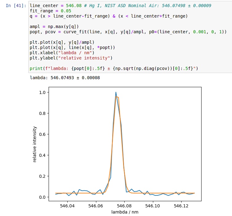
Here you can see the 546.075 nm mercury (Hg) line, which NIST ASD reports with 546.07500 ± 0.00010 nm, reproduced as 546.07493 ± 0.00008 nm by my spectrometer (source is an old “energy-saving” light bulb from the basement, those contained mercury). This result is within statistical uncertainity of the NIST value, and even has smaller statistical uncertainity than the literature value. The result has more than 8 significant digits.
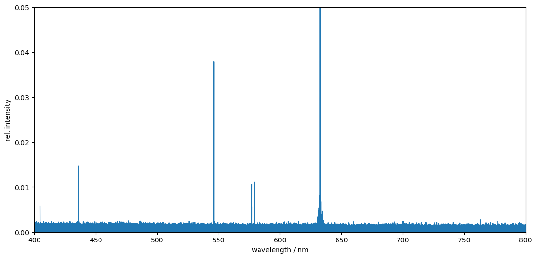
This isn’t a fluke either, the same spectrum this data was taken from covers the full visible range, and contains several such lines with similar accuracies (e.g. Hg 435.83363 ± 0.00010 nm from NIST ASD is detected at 435.83359 ± 0.00008 nm).
How this works? Read on to find out.
Project history
Before I continue, one paragraph of project history. This started as a joke toy project to build world’s worst fourier transform spectrometer. I then kind of got hooked and wanted to build a proper one, initially with the plan to sell the device as a for-profit enterprise. While the prototype I built worked and showed some pretty impressive results, I decided it to be too big of a task to productize it into something that would actually sell, and dropped the project. (We are commercially building Raman spectrometers now instead, which use simpler grating spectrometers.)
In this post, I want to document how the project went and show some results, since I think commercial use is quite unlikely by now and it would be sad to see the results disappear into the void without anyone ever seeing them.
Project goal
The goal of the project was to build a general-purpose, ultra-high resolution spectrometer for visible light, an optical spectrum analyzer. I originally envisioned with proper technology, this could achieve higher throughput and thus better signal-to-noise ratio than conventional spectrometers, which I learned to be a misconception during the project, though.
Project components
To build a fourier transform spectrometer (I will not go into detail again here how these work, please read my earlier post on the topic of the wiki article if you are interested), we need several non-trivial components:
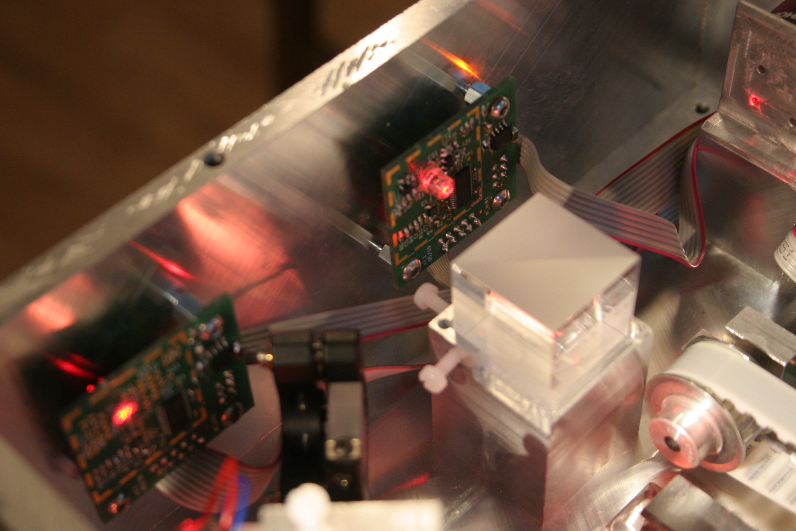
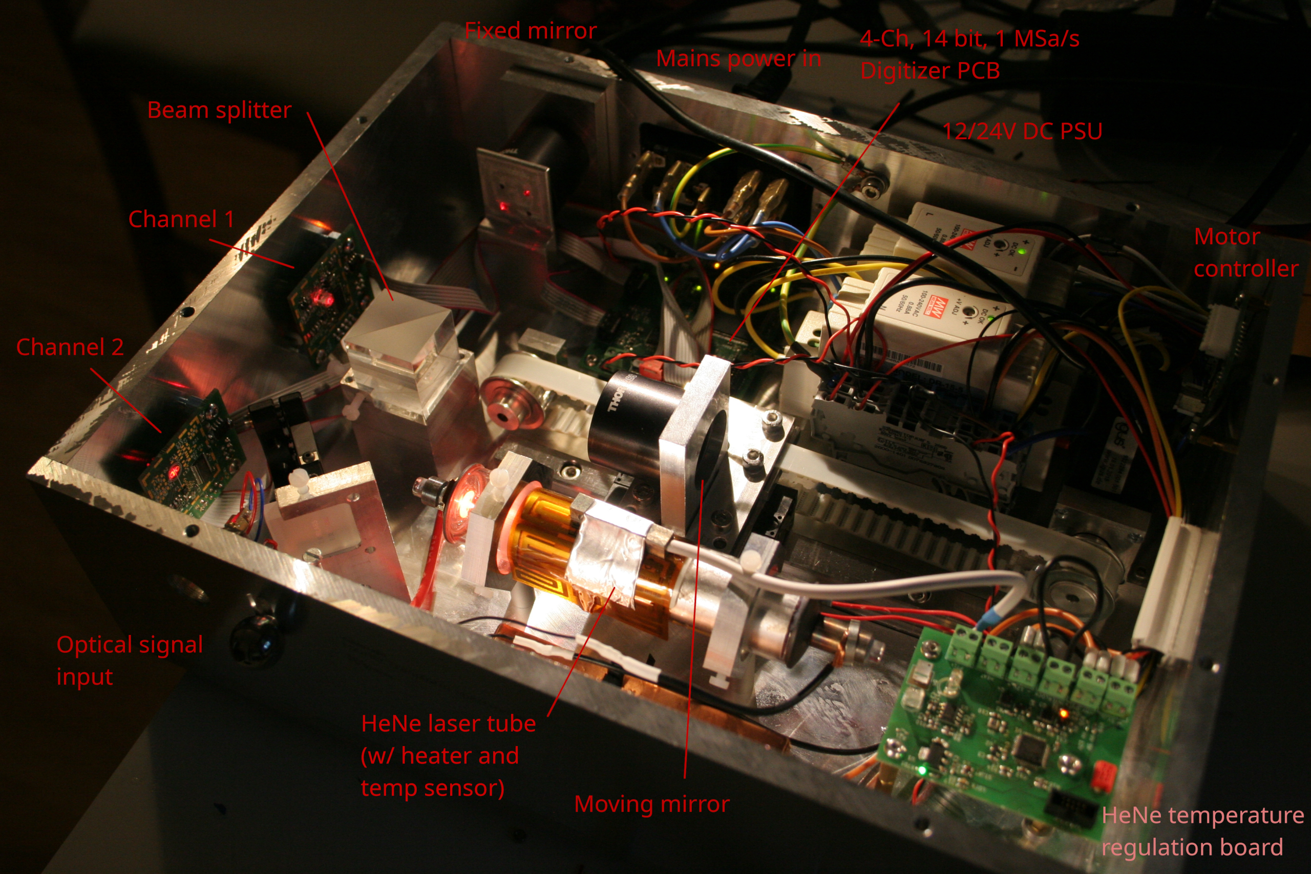
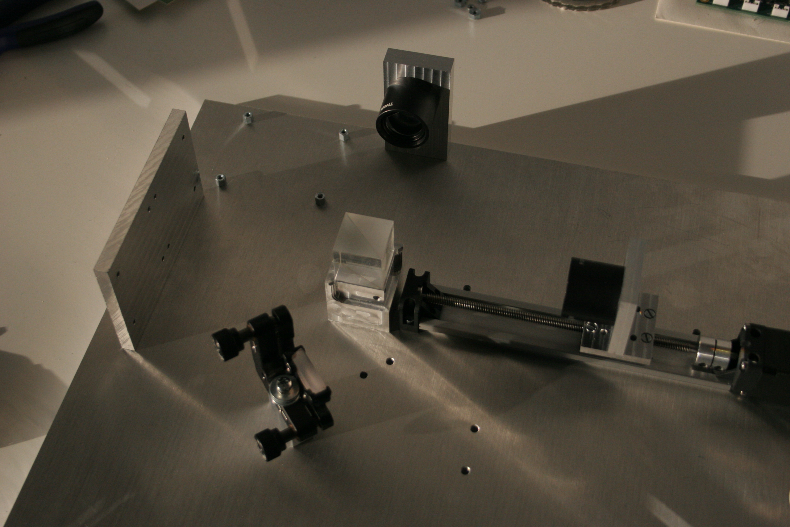
- A Michelson interferometer, consisting of a beam splitter and two mirrors.
- A rail which moves one of the interferometer mirrors back and forth, with several cm in length. (The length determines the spectral resolution.)
- Either position control or position sensing for this mirror, with < 100 nm (!) accuracy.
- A detector, like a photodiode. Ideally, this has 2 channels, since the interferometer has 2 outputs.
- A digitizer, which records the detector level as the mirror moves.
- Software which computes optical spectra from the recorded data using a Fast Fourier Transform algorithm.
In the following, I will describe how I designed built those components.
Michelson interferomter
For this, we don’t need much — just two retro-reflector mirrors, and a beam splitter aligned precisely. These components can be bought off-the-shelf. To get everything in place, I have a CAD model of the whole device, including the beam path.
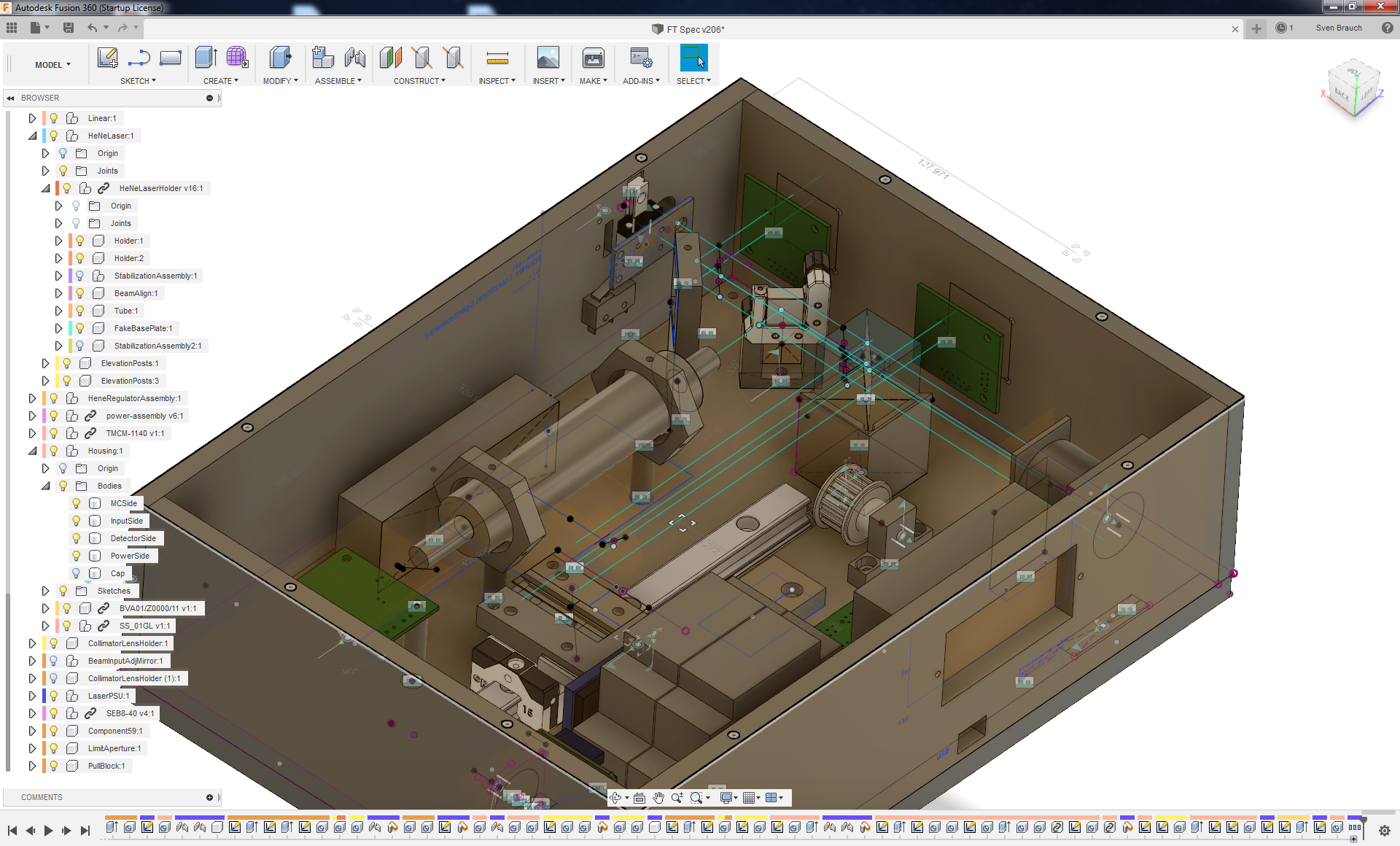
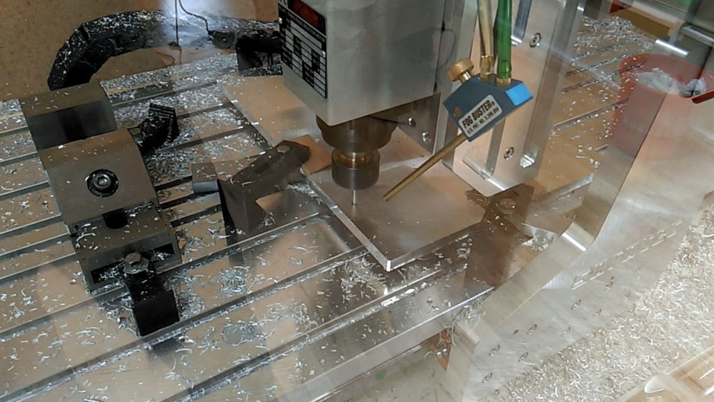
Each individual part is made from Aluminum on a CNC machine.
This is quite some effort, but it overall works well and the results are good.
10 cm moving mirror rail and positioning concept
Many commercial FT systems or ones mentioned in literature use position-regulated rails for their mirrors, meaning they have a closed-loop feedback system for positioning the mirror at a location accurate to ~100 nanometers. I decided against going this route, since it seemed unnecessarily complicated. We do not actually need to precisely position the mirror; it is sufficient to know where it was for each sample.
In my system, this is realized by adding a second channel, geometrically parallel to the measured light, into the interferometer assembly. Into this second channel, we inject laser light from a known-wavelength source. From this, we can compute the mirror position — more on that in the next section. For the mirror rail, what matters is that it does not need to be able to accurately position anything; it is sufficient if it moves the mirror in a straight line at a somewhat constant speed.
I ended up simply using a step motor with a belt driving a sled on a steel linear rail. This does have some backlash, but it’s simple to build and relatively cheap, and it is very stiff and precise in its movement direction.
Position detection system for moving mirror
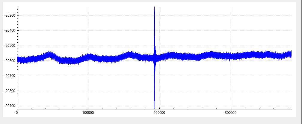
As explained in the previous section, a reference laser passes through almost the same optical path as the measurement light. This is a HeNe laser with a wavelength of 632 nm. As the mirror moves, we see interference fringes from this laser in a reference channel output — one light-dark cycle every 632 nm of optical path difference. By counting these fringes, we can calculate the position the mirror is at for each point in time.
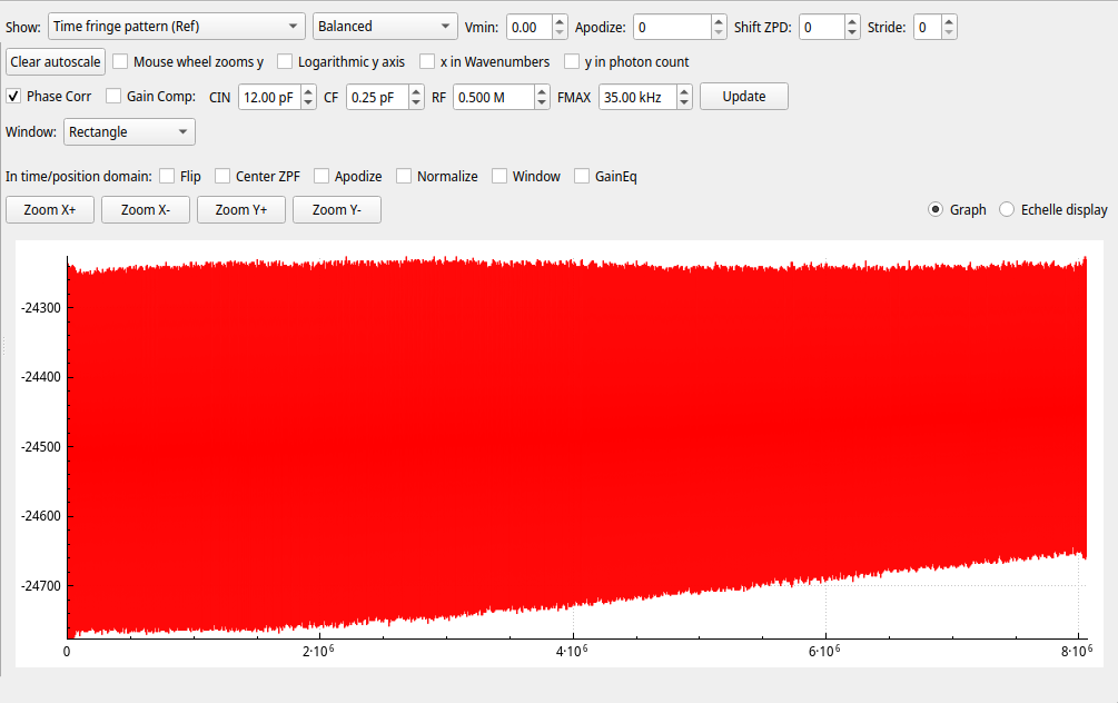
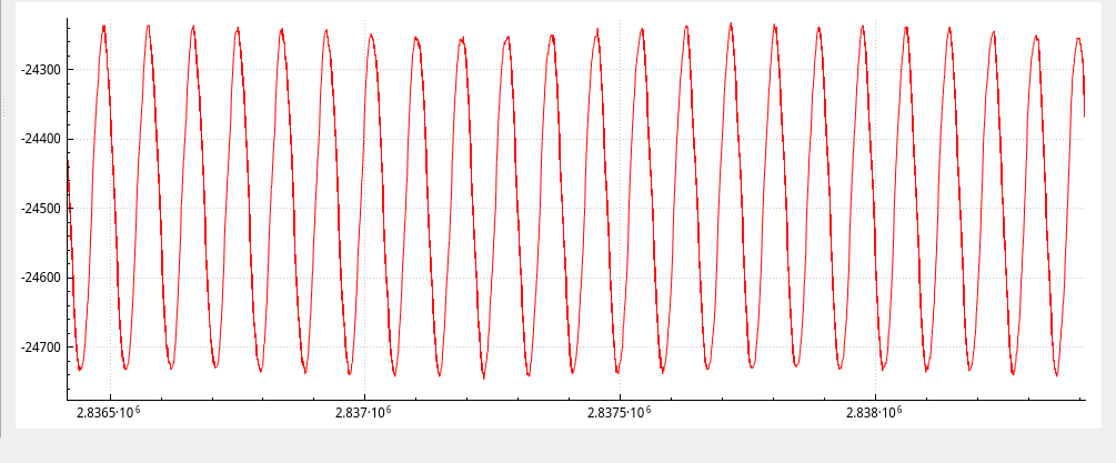
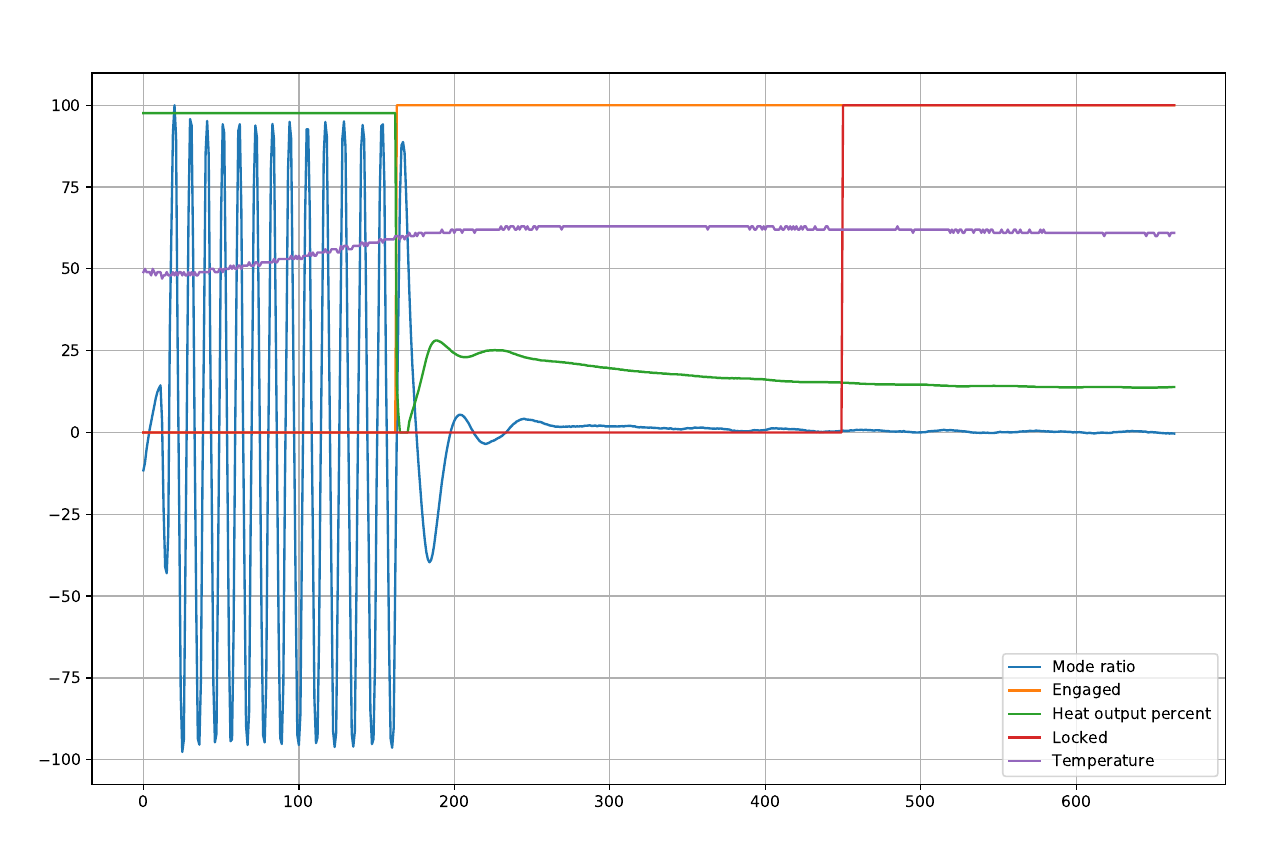
By counting these fringes, we can reconstruct a position curve and, as its derivative, a veolcity curve of our mirror. The position curve is quite boring, it’s visibly just a straight line; the velocity curve is more interesting:
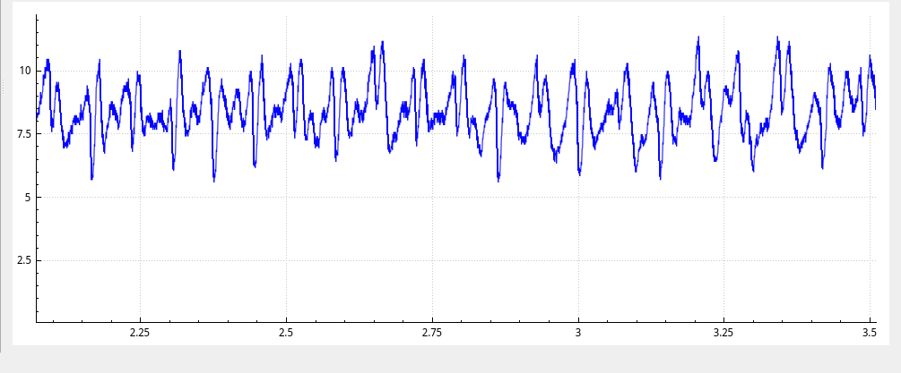
Here we clearly see some un-roundness from our motor drive. We don’t care though, we know from this data where exactly the mirror surface was positioned at each time, to an accuracy of probably < 20 nanometers. That’s all we need.
We can now use this data to re-sample the x axis of the actual measurement data, from “sample index” (i.e. time) to “optical path length difference in the michelson interferometer”.
The role of laser accuracy in this strategy
We have one problem now though: we need a laser with
- precisely known, stable wavelength, and
- sufficient coherence length, so it actually produces a nice fringe pattern across our whole 200 mm path length difference (10 cm rail equals 20 cm path length difference, back and forth).
Fortunately, one of the oldest known lasers can reasonably fulfill these requirements: The helium-neon laser.
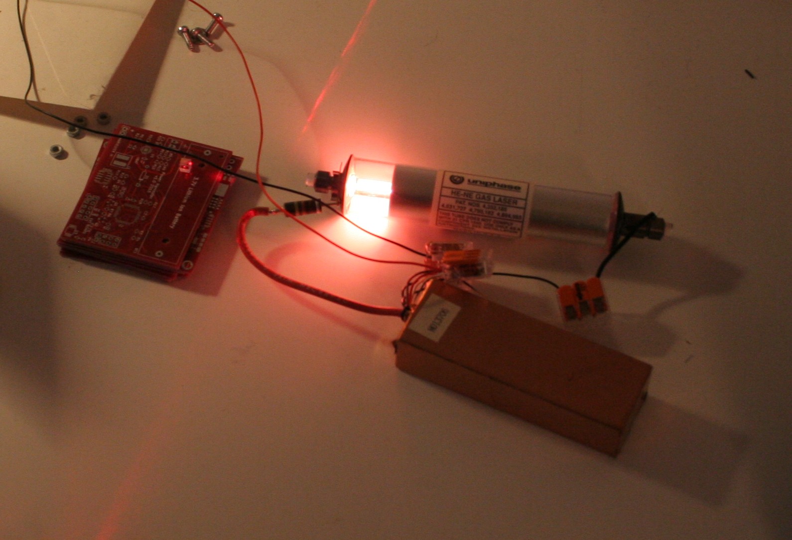
These are available used from various sources for somewhat reasonable prices (low three-digit euros range).
Such a HeNe laser in itself is not bad, but it can be even better when it is temperature-stabilized. This is a fascinating physics and engineering topic, worthy of an article on its own, but doesn’t really fit into the length of this post.
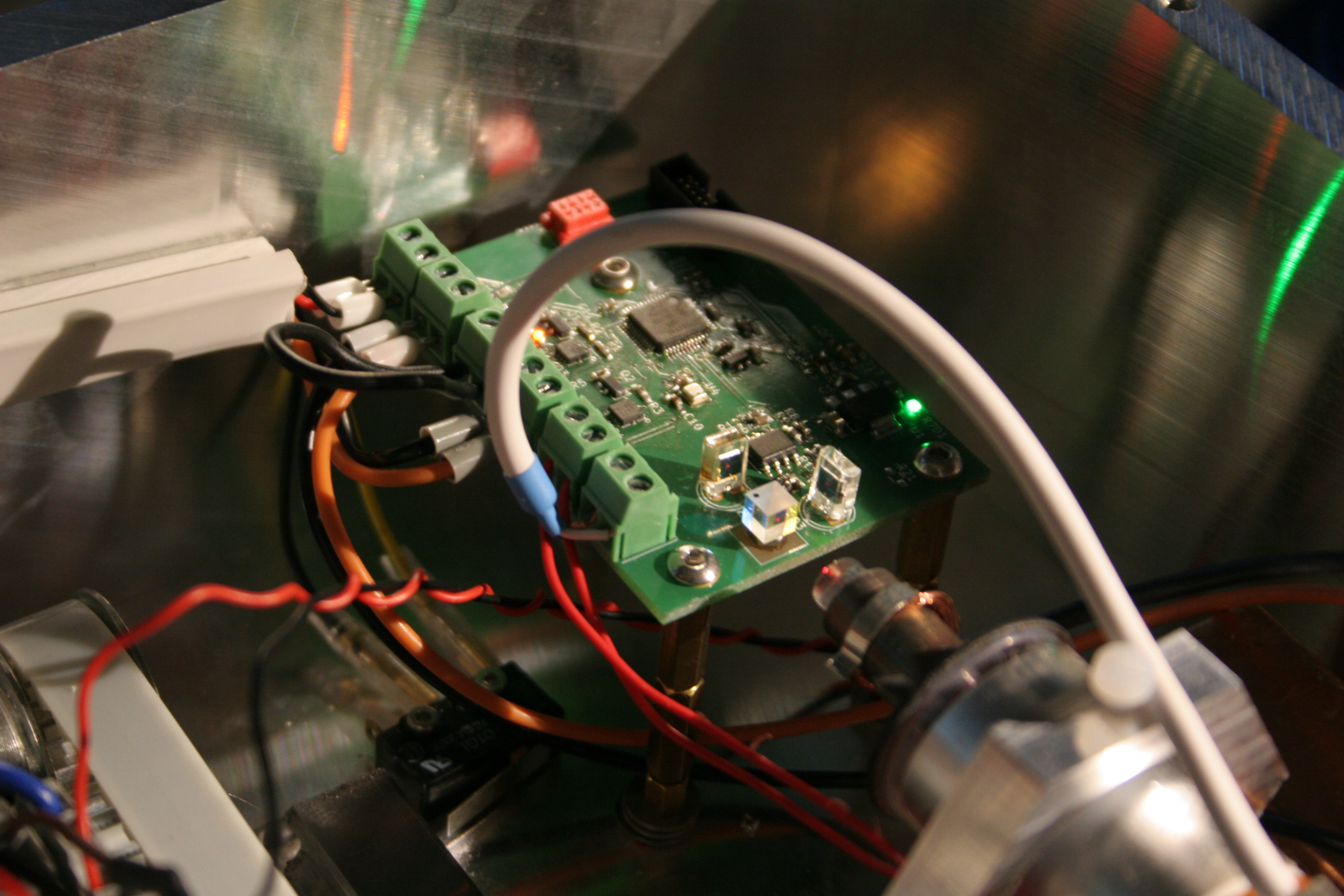
Suffice to say, by using a polarizing beam splitter and regulating the temperature of the laser tube such that both polarizations have equal intensity significantly improves accuracy and stability of the lasing operation. For this FTS, I designed and built a PCB with a tiny beam splitter, 2 photodiodes, a transimpedance amplifier, some FETs switching on and off a heating kapton foil wrapped around the laser tube, and a LPC1112 microcontroller implementing a PID engine in software to perfrom this regulation. A temperature sensor on top of the laser tube is used to speed up startup when first turned on (we can heat to a certain temperature below which we know stable operation cannot be achieved).
This gives us an ultra-precise, ultra-stable source for reference light, which amazingly covers all calibration requirements this device has.
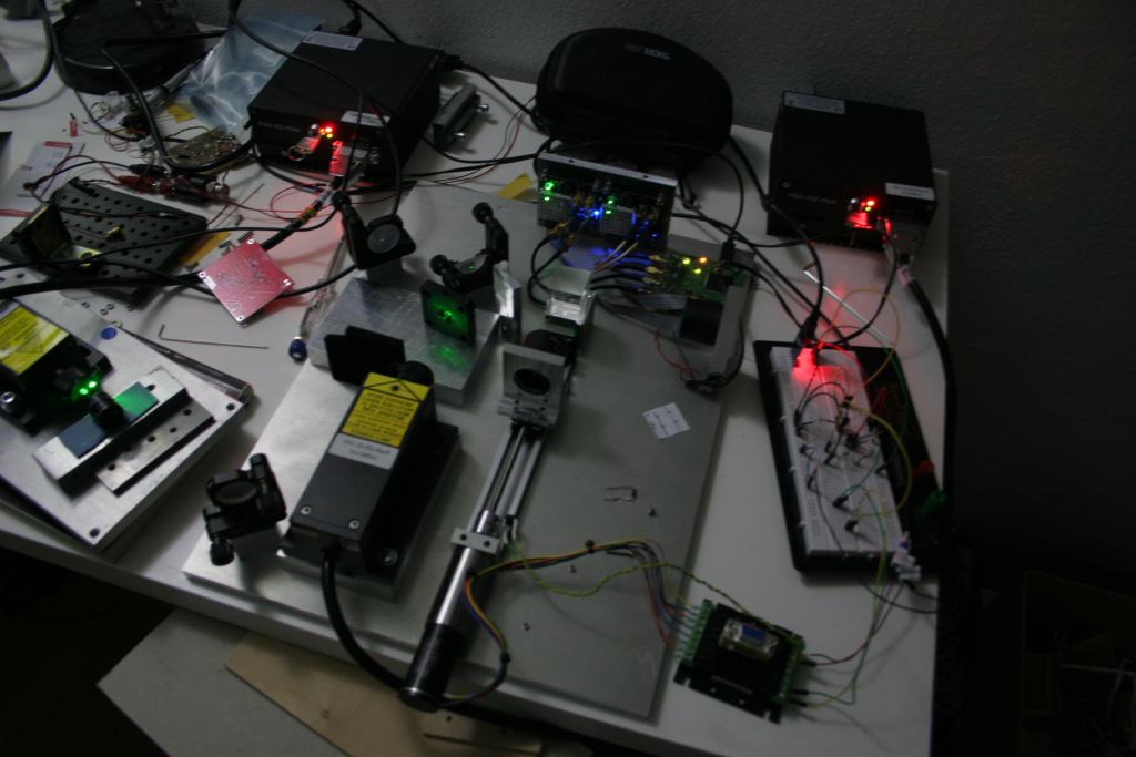
Detector circuit board
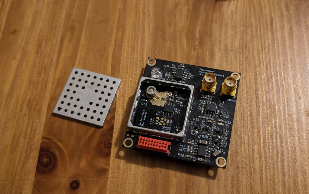
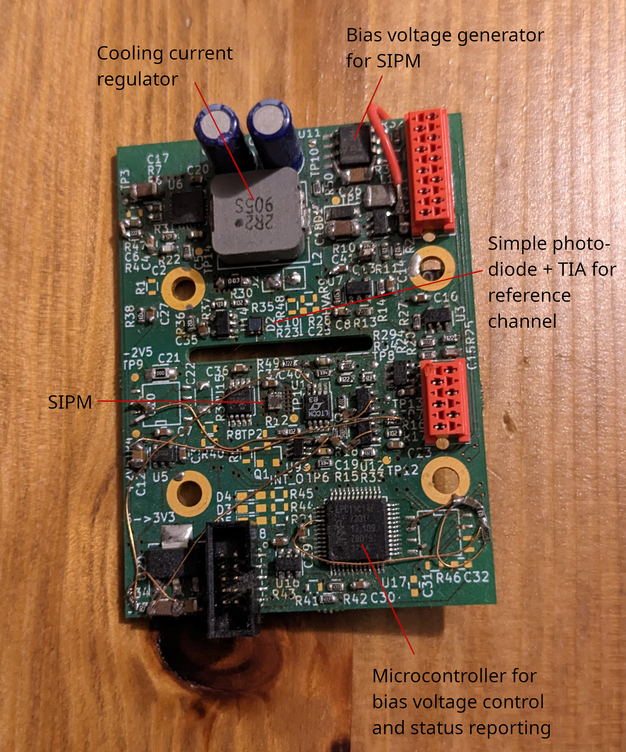
The detector circuit board needs to turn the light exiting the interferometer into an electrical signal. This board had several iterations; initially, it was a high-gain transimpedance amplifier, but later turned into a silicon photomultiplier board.
The main problem with the transimpedance amplifier is that its bandwidth gets really low at high gains. The gain curve is also not super flat, leading to artifacts in the spectrum when the mirror velocity is not constant. They are also super sensitive to environmental radio frequency interference; without the RFI cover depicted above, this board basically doesn’t work at all.
Silicon photomulitpliers, in contrast, are a new kind of technology which use large armouns of avalanche diodes in parallel to capture photons. They give outputs similar to classical photomultiplier tubes (PMTs), but with much smaller size, higher quantum efficiency, and lower voltages (my PCB uses ~40 V). Like PMTs, they have an intrinsic gain and do not usually need a separate amplifier circuit before the analog-digital-conversion. The gain can be controlled by changing the voltage on the device. This works really great and I’m very happy with this kind of detector.
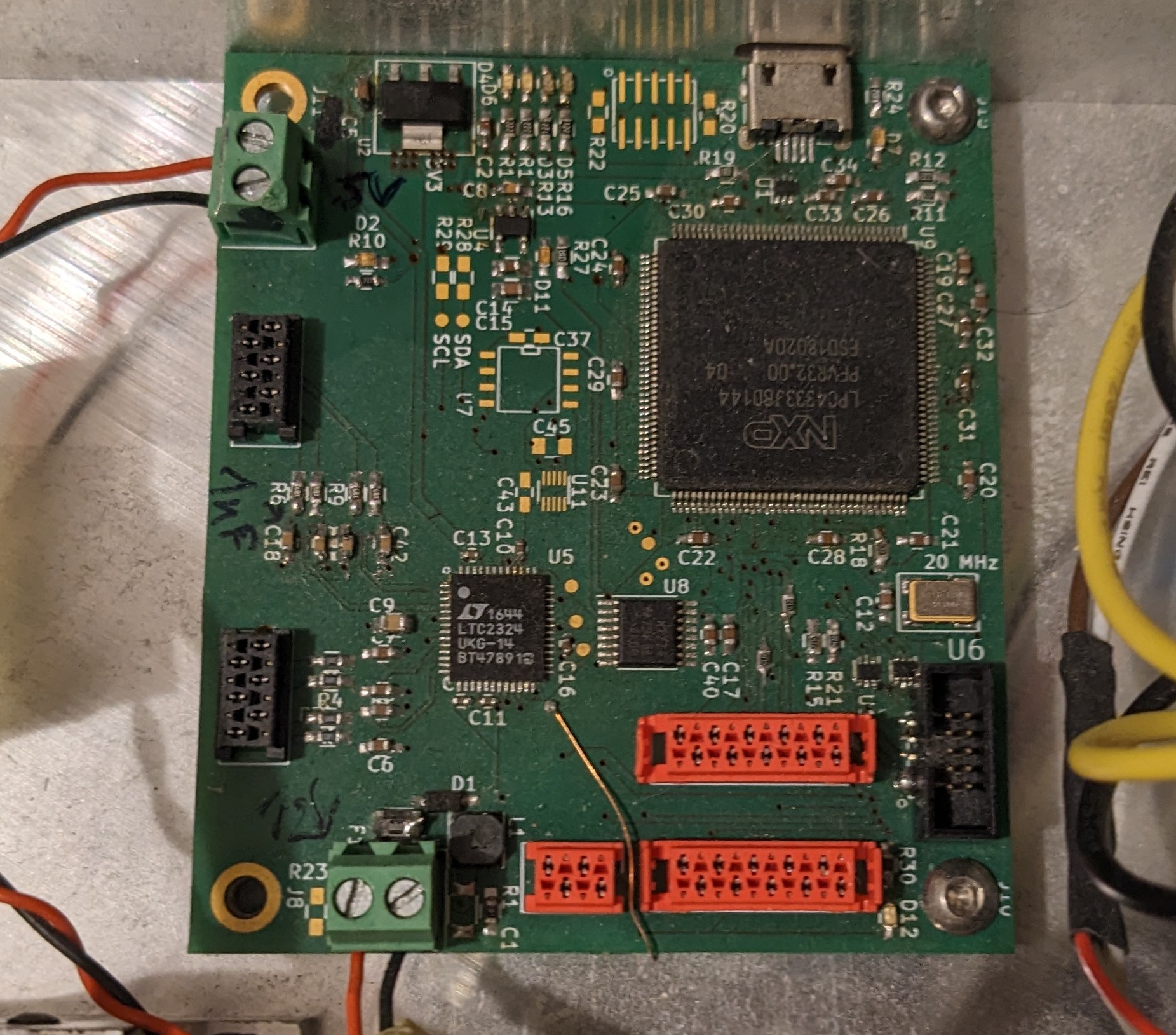
Digitizer circuit board
The digitizer printed circuit board (PCB) needs to simultaneously sample 4 analog channels (actual signal and reference signal from the HeNe laser, for 2 channels) with high-enough™ bit depth and sample rate.
What’s high-enough sample rate? If we move our mirror at a maximum velocity of 20 mm/sec, we will see 100.000 fringes (dark/bright changes in the interferometer output) per second at 400 nm wavelength. Nyquist’s theorem says we need a sample rate larger than 200 kHz for that, but to be on the safe side and for easier debugging, I went for 1 to 1.5 MHz.
What’s high-enough bit depth? Well, this very much depends on the signal. With perfect gain control, for this application, you will need very few bits. 2 bits would probably be totally fine and yield perfect spectra. However, we don’t have perfect gain control. Our input signals might have very different amplitudes, and the amplitude of the interferometer output might even vary during a sweep.
Thus, I went for a generous 14 bits, which drastically reduces requirements on the signal preconditioning before it reaches the ADC.
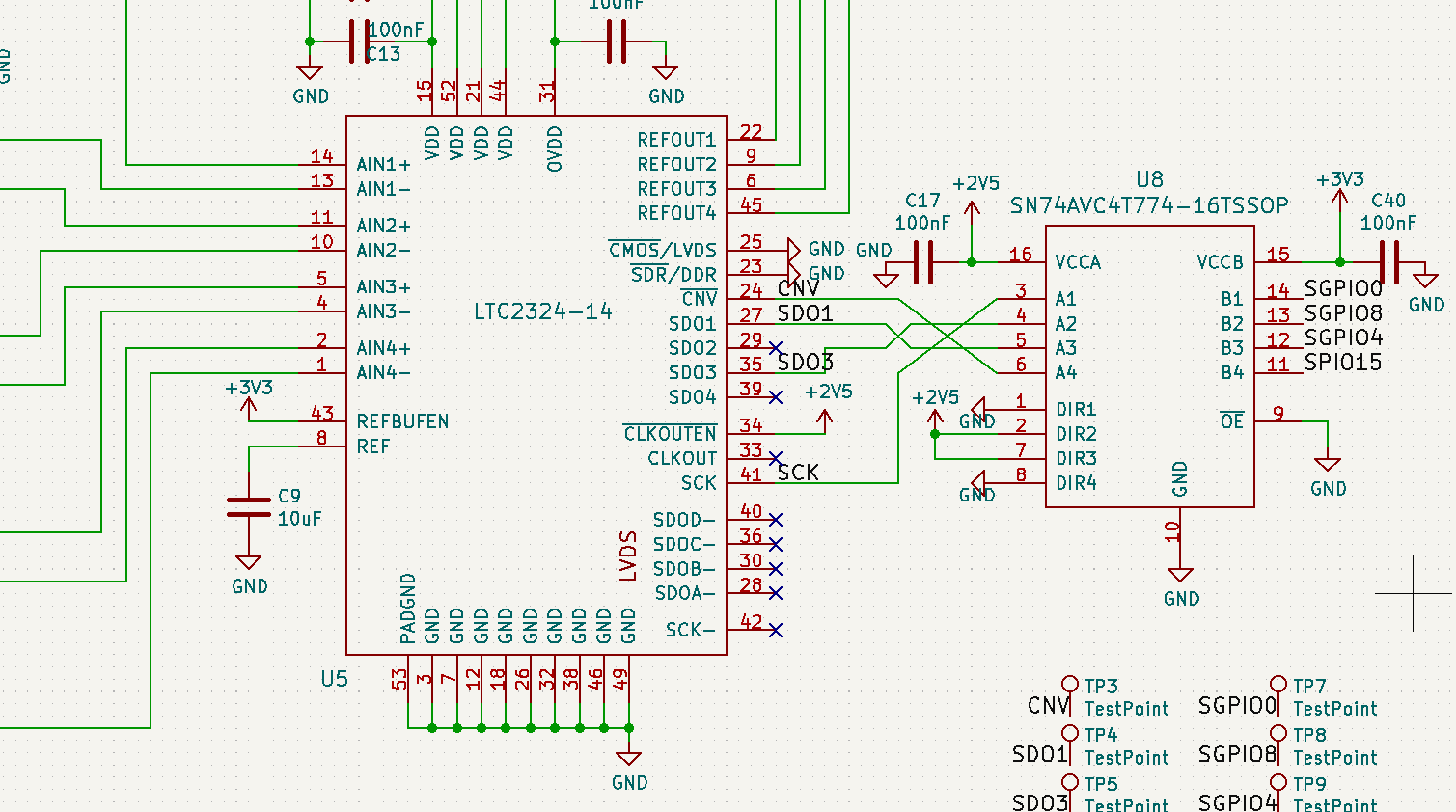
The digitizer PCB I designed for this project features a LTC2324-14 four-channel, 2 MHz, simultaneous-sampling 14-bit ADC, controlled by a LPC4333 microcontroller. This part actually has 4 ADCs, not just 1 or 2 ADCs connected to 4 outputs with a multiplexer; we need this because we want to sample all four channels at precisely the same times.
The microcontroller firmware then uses the LPC4333 SGPIO hardware module quite extensively to implement the timing diagram for talking to the LTC2324-14. The SGPIO module features various shift registers and I/Os which can be chained together with a lot of configuration options. This was quite challenging, as clock speeds of around 50 MHz are involved to retrieve data from the part quickly enough — not easy to do with a 200 MHz clock speed CPU. (I’m a little bit proud of this.)
But ultimately, this works nicely; the microcontroller acquires the samples (about 12 MB per second!), packs them, and streams them to the PC host using high-speed USB.
This board also has some other duties, such as talking to the laser controller and motor controller via CAN bus, relaying the host software’s commands to them and reporting their status to the PC.
PC Software
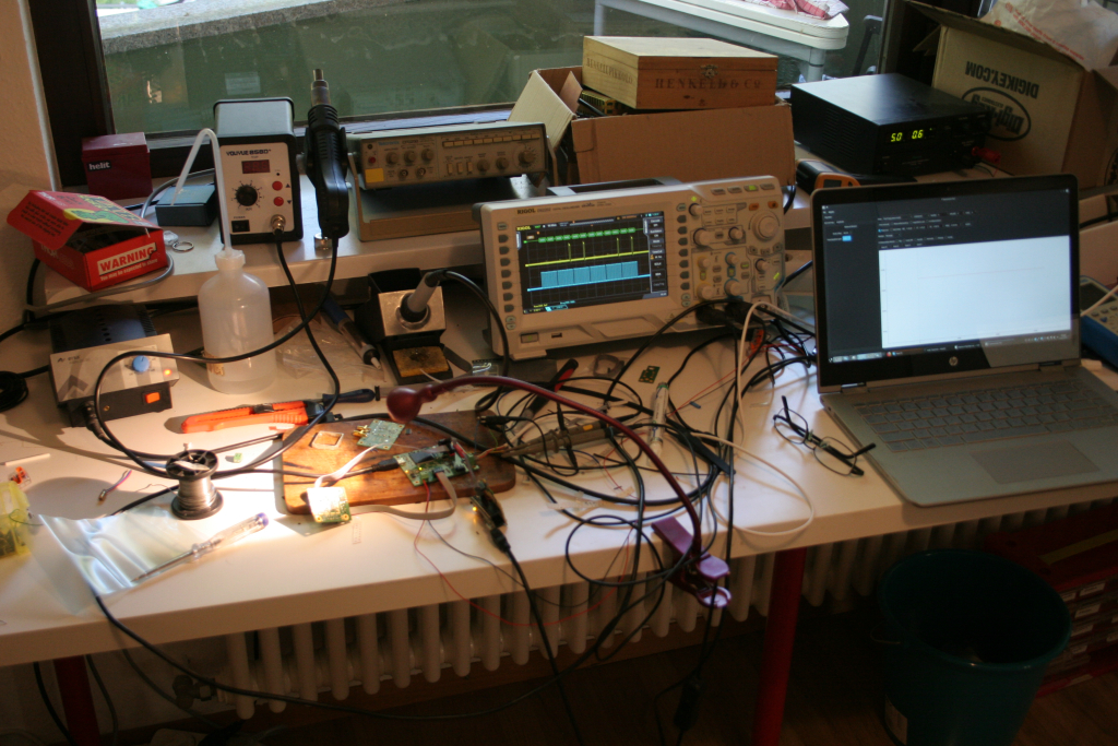
The PC software implements the communication protocol with the digitizer board and controls the whole device by talking to it. It uses libusb to do this. It also displays the results, using Qt and the Qwt plotting toolkit. (It is of course 100% a development prototye / tool and would never reach an end user any way like this.)
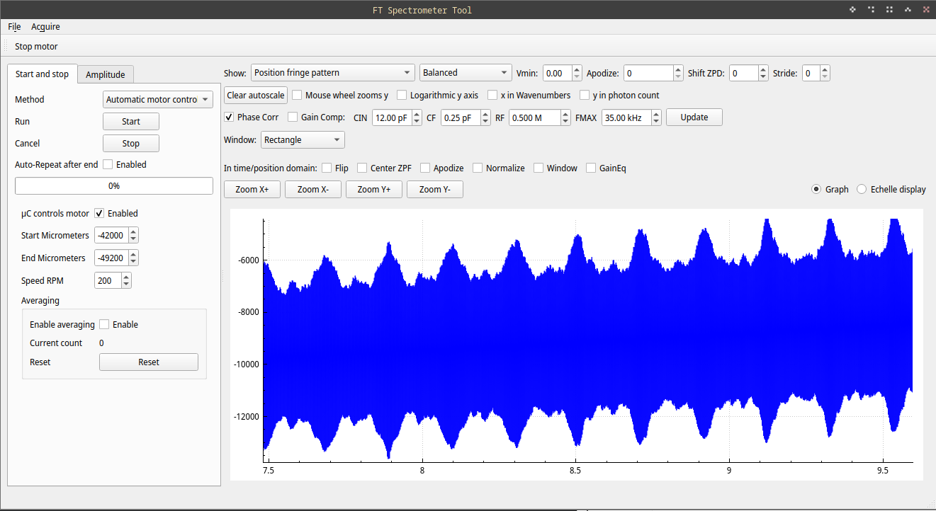
It also implements all the logic and algorithms required to obtain optical spectra from the raw samples. This isn’t super complicated, but there are still quite some steps involved, such as identifying the reference fringes, counting them, computing the mirror position, re-sampling the measurement data from time to the mirror position, combining the balanced and unbalanced interferometer outputs, centering the zero-position fringe (important for white-light spectra), applying a windowing function, and finally computing the actual fourier transform.
And this, finally, is everything needed to get the super-precise measurement presented in the opening paragraph.
That’s it! I hope this was at least a bit interesting to read. It definitely was very interesting to build.
Categories: Everything