Much has happened since my last status report on my attempts to observe the galactic hydrogen emission at the famous 1420.4 MHz hyperfine structure line. Now, the new setup is finally proven to be basically working, and in this post I want to describe some of the changes I did.
New data acquisition module
Most importantly, I replaced the spectrum analyzer by a self-made data acquisition unit which is basically a Software-defined radio (SDR). Its purpose is to take the 1.4 GHz signal, digitize it, and send it to a computer.
Functionality description
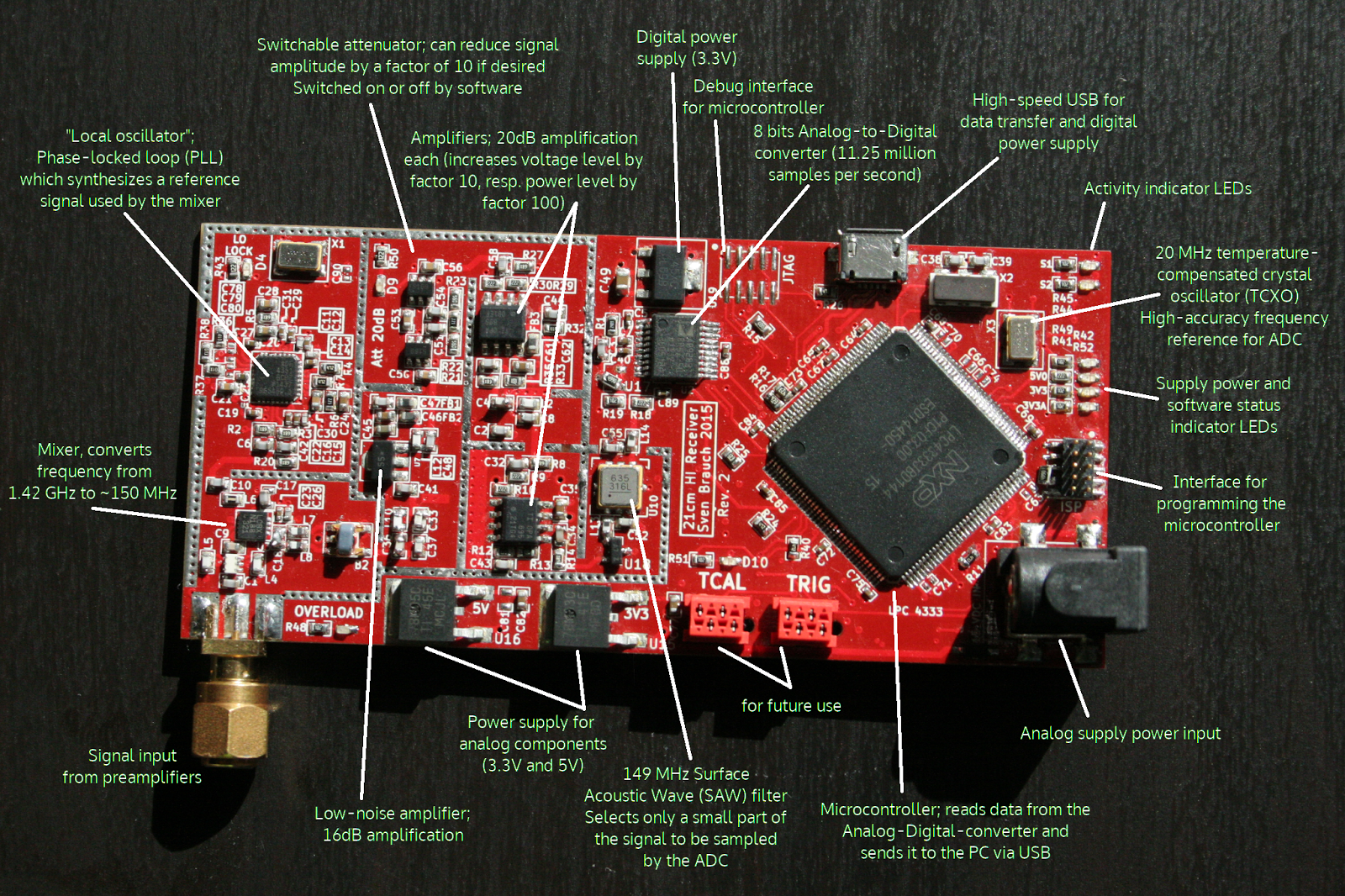
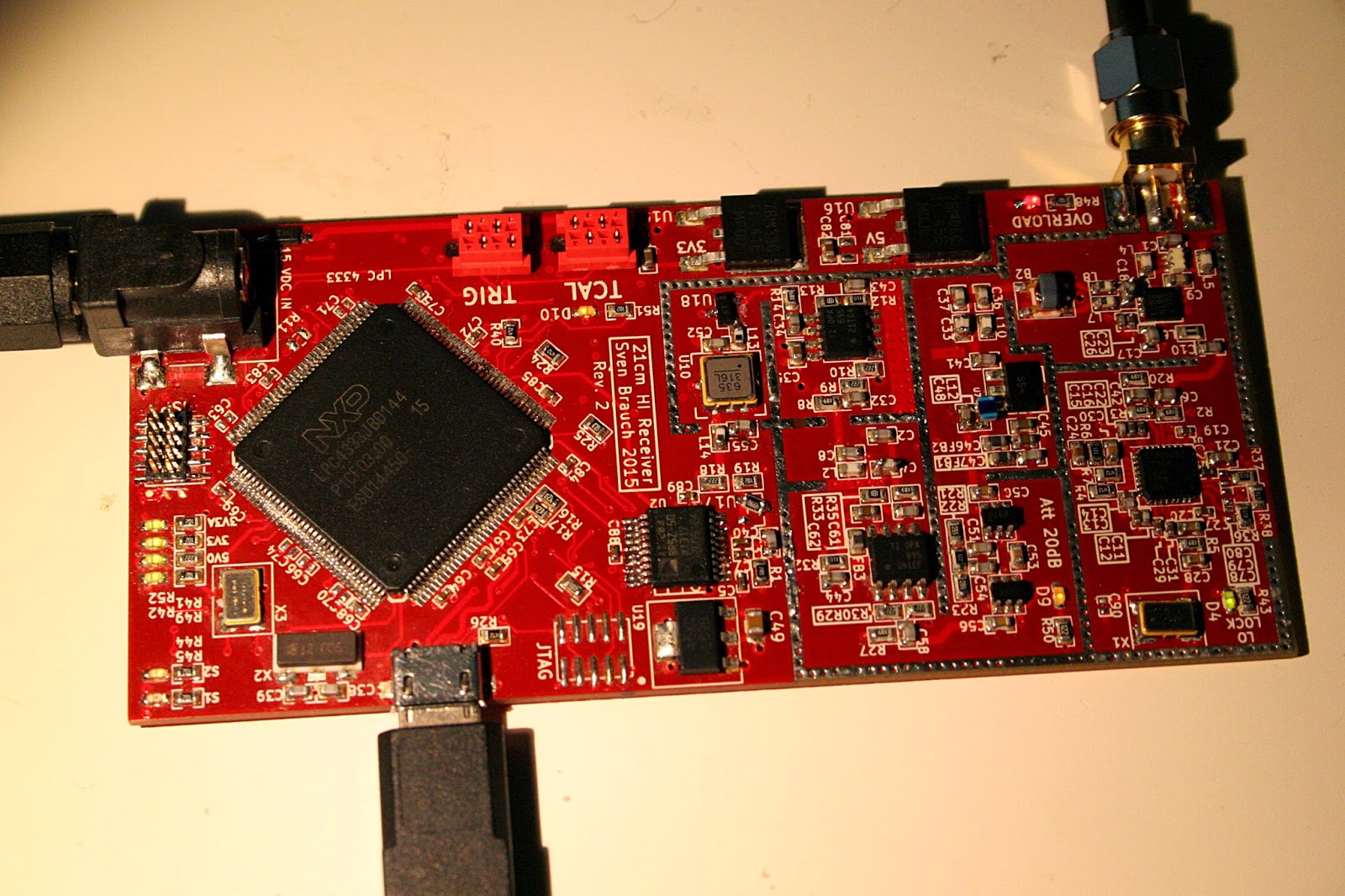
The board contains various submodules, most of which are labelled in the following image.
 |
| Some of the components of the acquisition board. |
The first thing which happens is down-conversion through a so-called mixer [data sheet of part used here]: it takes the portion of the 1.42 GHz signal we are interested in and moves it down to a lower frequency of approx. 150 MHz. This has various advantages; especially it makes further filtering, amplifying and digitizing the signal much easier. Since we are only interested in a small part of the signal, this conversion can happen in a way such that no information is lost.
Mixing works by multiplying the actual signal with a reference signal, the so-called Local Oscillator (LO) [data sheet of part used here]. You can imagine the LO as a component which generates a sine wave at a specific, but programmable, frequency (in this case around 1.27 GHz); then the mixer basically subtracts this frequency from the frequency of the original signal (so in this case, with 1.42 GHz and 1.27 GHz you end up at 0.15 GHz = 150 MHz). The lower-frequency signal (the 150 MHz in this case) is called the Intermediate Frequency (IF) signal.
Next, there are various filters and amplifiers which are very simple to understand; they just make the signal amplitude large enough so that it can comforatbly be detected by the analog-digital-converter later on.
This part of the circuit ends with a so-called Surface Acoustic Wave (SAW) filter [data sheet of part used here], which is a quite modern kind of filter with the special property that it can select a relatively small part of the signal very accurately, while blocking everything else almost completely. It only lets the frequency components of the signal pass which have frequencies between about 148 and 151 MHz. Which part of the original signal can be found in this range (remember, we move the original signal to a different frequency) is determined by the mixing step: through programming the local oscillator (LO) for a different reference frequency, one can look at the input signal’s spectrum one part at a time.
The bridge between the analog and the digital world is built by the Analog-Digital-Converter (ADC) [data sheet of part used here]. It gets an input clock from the microcontroller, which is just a signal which toggles up and down exactly 11.25 million times per second; on each tick of that clock, it measures the voltage at its input pin, and converts it into an 8-bit digital value. Each of the bits of that value is then provided as a voltage level (either +3.3V for “1” or 0V for “0”) on one of the output pins. They are read in by the microcontroller [data sheet of microcontroller], packed into chunks of a few kB in size in the controller’s RAM, and then sent out via USB.
Getting the microcontroller firmware to do this as fast as required was surprisingly nontrivial, but that’s such a broad topic that I do not want to get started on it here.
The computer receives the data, calculates the fourier transform to get the frequency spectrum, and averages the resulting spectra (see end of post for software screenshots).
(If you ever heard of the Nyquist frequency, you might wonder how it is possible to digitize a 150 MHz signal with just 11.25 MSa/s sample rate. This is why we need the narrow SAW filter in front of the ADC: it limits the bandwidth of the signal to 3 MHz and thus allows to use the undersampling technique. In this case, the ADC samples the 26th alias of the original signal.)
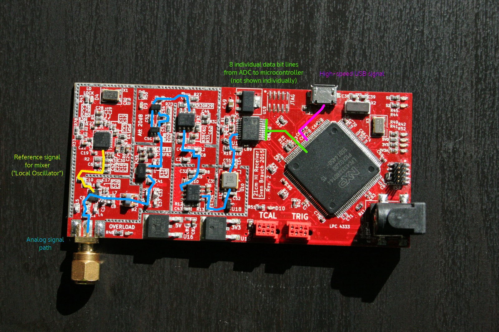
Below is an illustration of the paths the signals described above take through the board. Note that almost all of the blue path is at 150 MHz; just the first centimeter up to the small black mixer IC is at 1.4 GHz.
 |
| Signal paths in the data acquisition board. |
Manufacturing the board
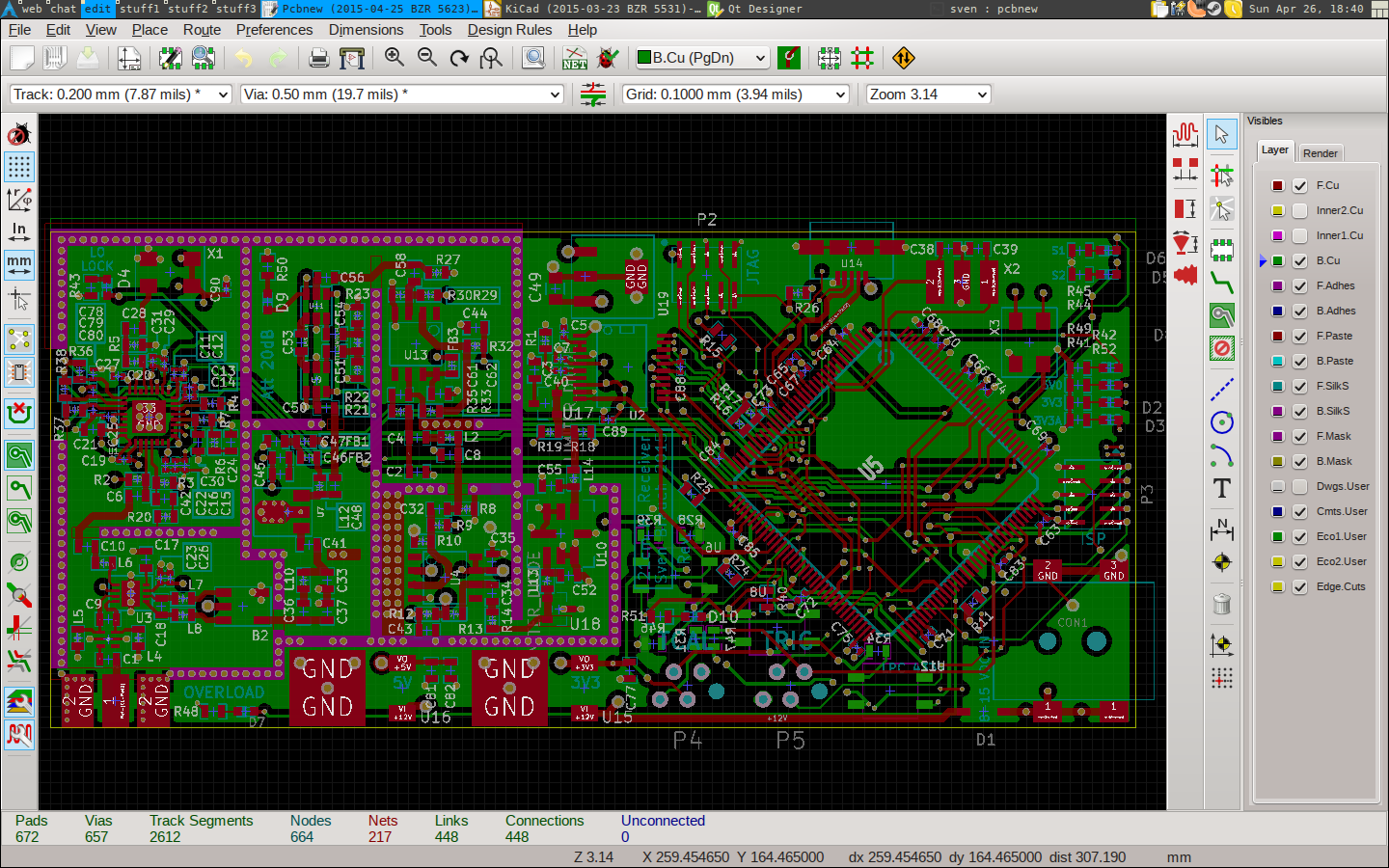
This is a 4-layer board; that means, it has tracks on the top and bottom side, and two metal layers in between (you cannot see them, they are glued inside the board) which also have tracks. Connections between the layers are established by metal-filled drill holes (in this case about 1000 of them, each 0.3mm in diameter).
Having 4 layers makes it much easier (or possible at all) to arrange tracks in a way that they do not cross, and also has some important advantages for high-frequency signals. Unfortunately, it also makes fabrication of the prototypes more expensive. There are various chinese vendors which will manufacture a small amount of pieces of such a board for an affordable price; including customs and shipping it will end up costing about 100 € for 5 pieces (less pieces doesn’t get cheaper though). Components are extra and you have to put them on the board yourself.
There is specific software to design such circuit boards; first, you usually draw a schematic, and then you use the layout editor to place components and tracks in accordance with the schematic. The layout itself quickly becomes hard to overlook; the software guarantees electrical equivalence between the easy-to-read schematic and the layout (e.g. it guarantees you don’t have wrong connections, missing connections, or tracks which cross or are too close together — of course only if you did it right in the schematic).
The software exports vector-graphics like files for each layer and a list where holes must be drilled, which is then sent to the manufacturer.
 |
| This board’s layout loaded in kicad. Only the top (red) and bottom (green) layers are shown. |
 |
| A raw board without components (but with soldering paste on it) and the stencil for the board. Also an example for how not to use a stencil. |
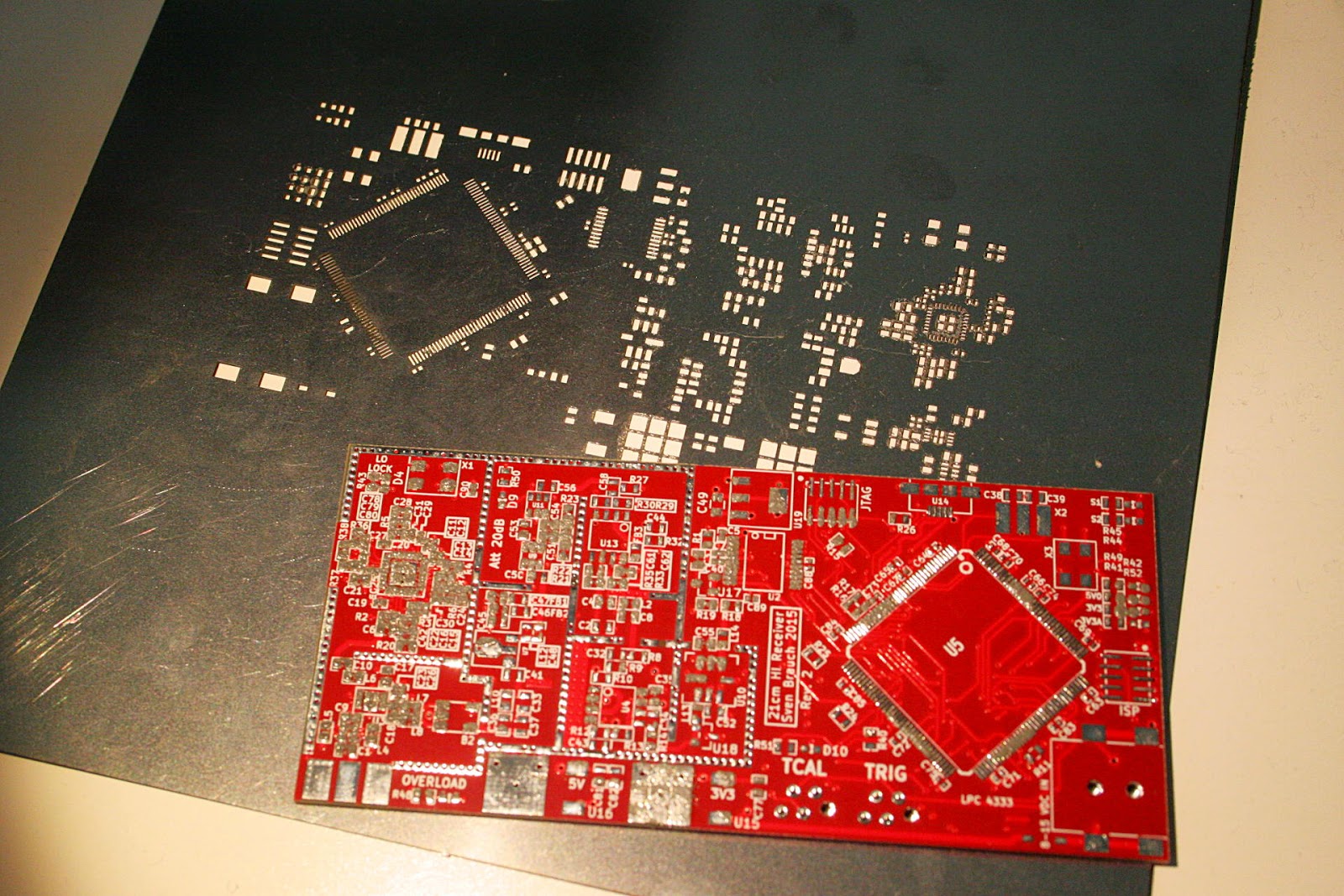
For this, I decided to use a stencil this time, which is a rather thin piece of metal with all the pieces cut out where a component is supposed to be soldered onto the board. The stencil is put on top of the board, then you smear some solder paste on it, and force it through with a credit card; then, you lift off the stencil to only have the solder paste on the places where it belongs. You can then put the components into their spots and heat the whole thing; the solder paste will melt and form a firm, electrically conductive bond between the component and the pad on the board after cooling down again. After a few attempts, I managed to get a good result for the paste print: it is important to firmly fix the stencil in the right postion, then press the paste through with a single swipe, and then remove the stencil again by lifting it straight up carefully.
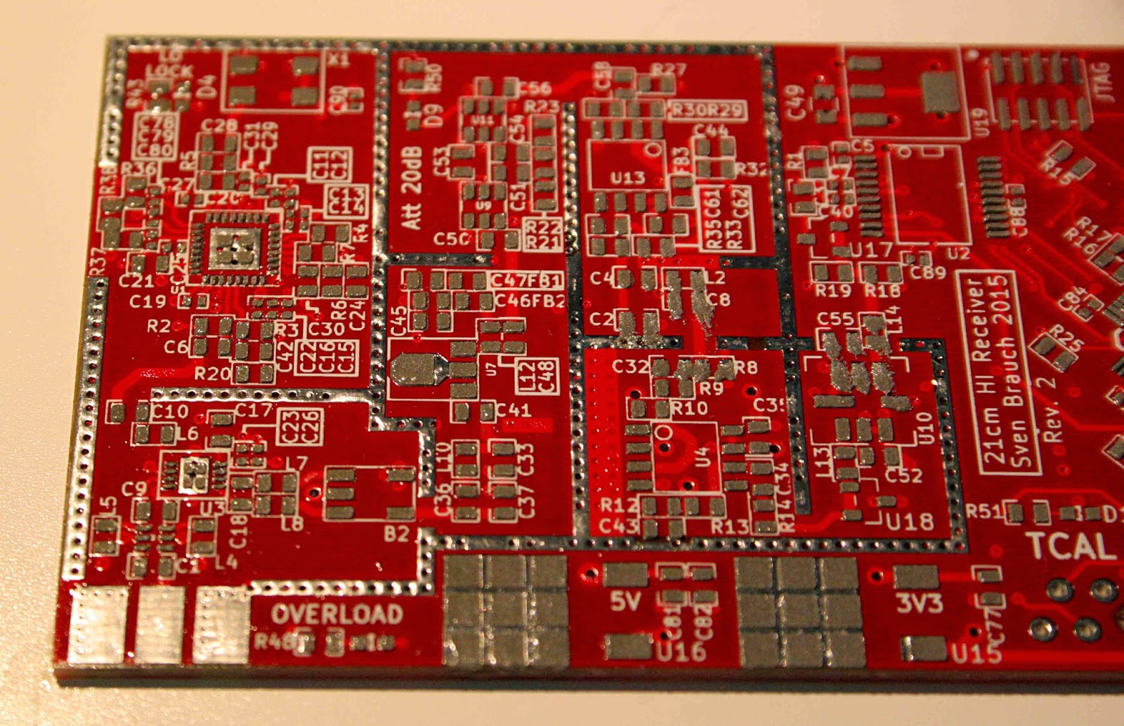 |
| Board with solder paste, ready for component placement. |
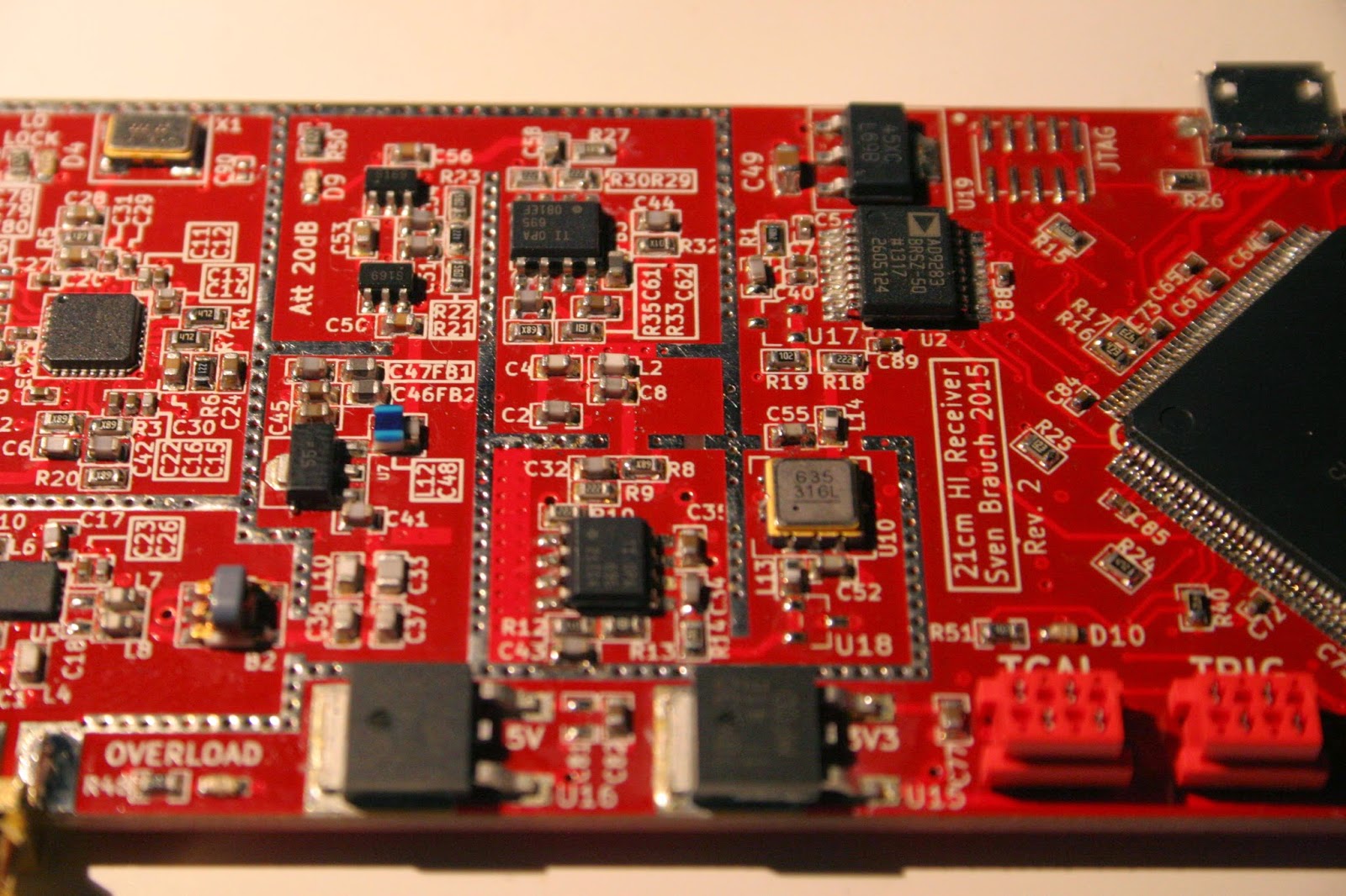 |
| Board with components placed, after heating it up and letting it cool down again (and fixing a few things by hand). Most of the solder joints look pretty good. |
With all the software and tooling stuff already in place from a first version of the prototype, it was quite easy to get this board to work as expected. Only very few minor fixes were needed.
Mirror filter
When mixing a signal to a different frequency as described above, there is one problem I did not mention so far: if I mix 1.27 GHz with a broadband signal (as it comes from the antenna, it doesn’t only contain the 1.42 GHz part but lots of uninteresting noise at basically all other frequencies as well) of which I am interested in the 1.42 GHz part only, there are actually two frequencies of the broadband signal which will end up at 150 MHz in the intermediate frequency (IF) signal. This is the 1.42 GHz = 1.27 GHz + 0.15 GHz part I want, but also the 1.12 GHz = 1.27 – 0.15 GHz part, which I have no interest in. After the mixing step, those two signals are added together and cannot be separated again. It is thus necessary to remove the 1.12 GHz part of the signal before it reaches the mixer.
To do this, a bandpass filter is needed. I did some simulation with Sonnet (give it a try if you want to do stuff like this, it has a quite functional free version), which basically allows you to simulate electromagnetic waves in planar (i.e. “mostly 2D”) arrangements of metal, and ended up with this magic-looking design:
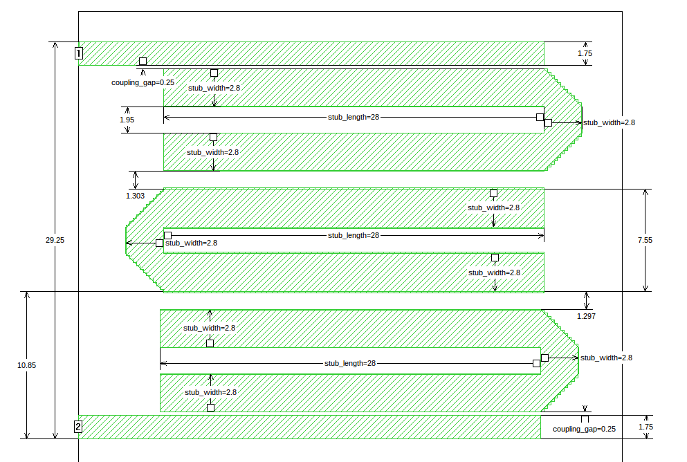 |
| Geometry for a microstrip bandpass filter at 1.42 GHz. |
The green stuff is copper, white is just board material, and the 1 resp. 2 is the input / output port. This is the simulated filter response:
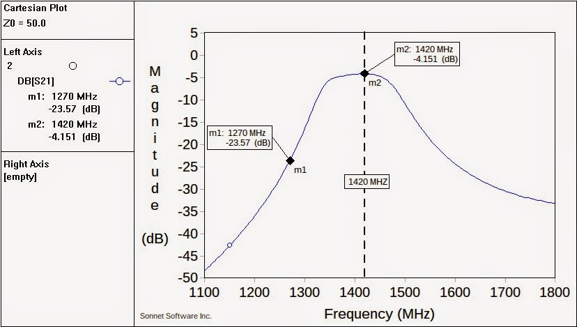 |
| Simulated filter response for the optimized design. |
Looks good! It lets through the 1.42 GHz signal nicely, and blocks the unwanted signal at 1.15 GHz by 40 dB (factor 10000 in power).
For a prototype, I then proceeded to cut this geometry into a copper board by hand …
 |
| Hand-made prototype (with a cutter knife). |
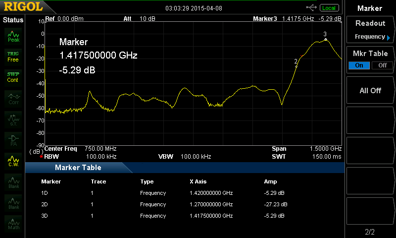
… and measured it to compare with the simulation. As expected, it has more loss in the passband than in the simulation (reality always has more loss than expected) but not much, and the shape of the response is much more irregular, probably mostly because of manufacturing inaccuracies. Still, the important parameters agree really well with the simulation, which I find quite impressive.
Astronomy
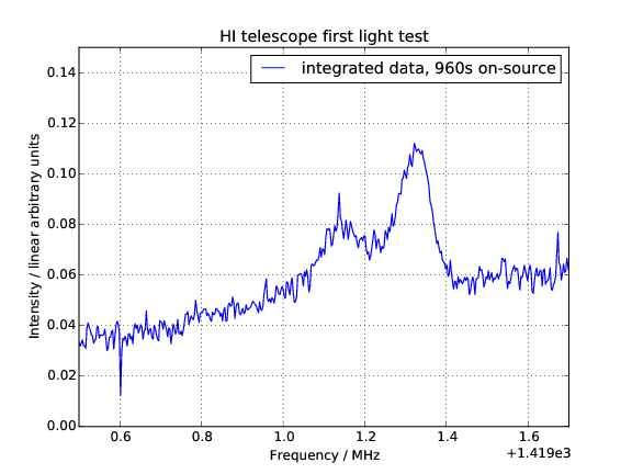
Now, finally all the important components are in place! I set up my 1.2m dish and pointed it at the sky, and tadaa — the familiar HI signature of our galaxy showed up:
I really need to repeat this test outside of a city full of people with interfering electrical devices (that really makes a huge difference), but as a proof-of-concept, this is completely sufficient. As such, this is the first spectrum I acquired with all significant components in the reception chain made by myself 🙂
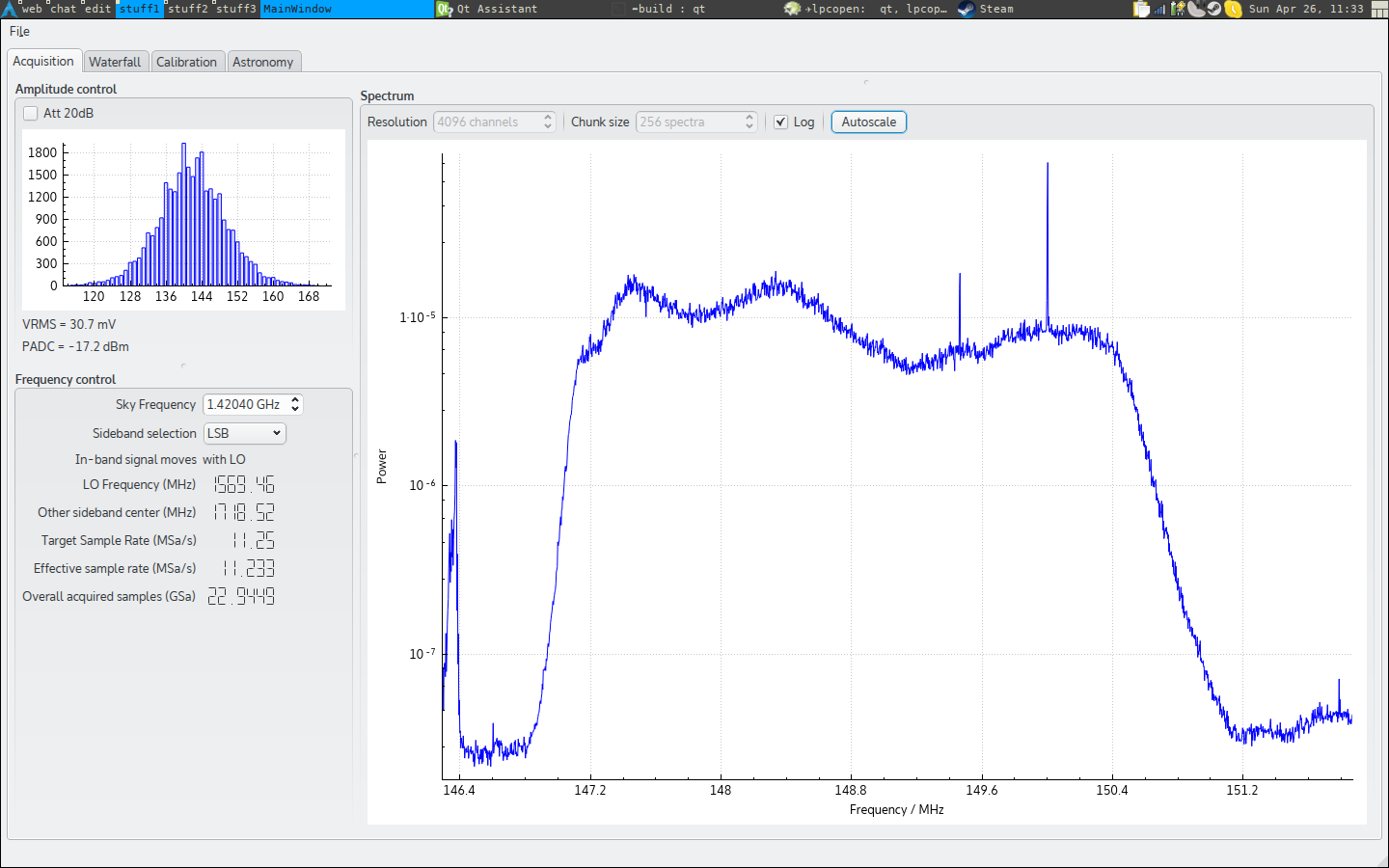
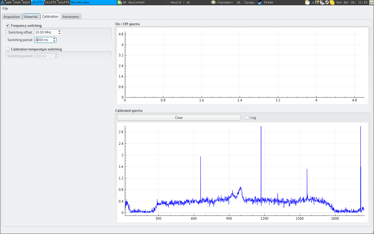
The signal is calibrated by a method called frequency switching: one periodically shifts the observation frequency by a few MHz, and thus observes just the background noise. This background noise is then subtracted from the actual measurement. This might sound like it reduces noise (it does not, but that’s not trivial to understand), but the real gain is that the frequency dependence of the IF part of the acquisition board is removed from the signal. Why this is important may become evident from the following image:
None of the peaks shown there is an actual astronomical signal; the signal shown in the plot is far too weak to see it here. The non-flatness of the band is created by the bandpass filter (the sharp spikes are interference); this non-flatness should be calibrated away in order to reliably distinguish real signals from the bandpass shape.
As you can see, the bandpass shape is removed, and the actual astronomical signal is visible in the middle (this is already averaged for a while, though).
Another interesting thing is to look at the waterfall plot of the record, i.e. encode signal intensity by color, and use the y-axis for time instead:
 |
| Waterfall diagram of the acquired signal. |
The relatively faint green vertical stripe around x=1000 is the signal we are looking for. Other vertical stripes are narrow-band interference; horizontal stripes are temporary but broad-band interference.
Next steps
The next thing I will try to do is build another of those boards, and do a bit of interferometry. Stay tuned!
Categories: Everything
Tags: astronomy, electronics, hardware, hydrogen line, radio telescope, soldering

That is so awesome Sven!
Could I interview you for the Astrophiz Podcasts?
It would be a 20min Skype chat at a time convenient to you.
https://soundcloud.com/astrophiz
Cheers,
Brendan
Why not, I’m not sure if I have anything interesting to say, but maybe if you ask the right questions 🙂
My spoken English is not terribly good, though. If you like, feel free to contact me by email: mail at svenbrauch dot de
Cheers, Sven
Hello, I am also very interested in radio astronomy and have been doing research on building my own SDR for 407mhz/1420mhz/10000mhz. Im currious why you decided to build your own radio to start with instead of buying an off the shelf SDR and adding an RF front end? I applaud the DIY spirit.
As far as the radio itself goes, why did you use an 8 bit ADC and undersample, when the NXP43xx has pretty high speed 12 bit ADC peripherals? Do you ever plan on releasing your hardware files, firmware, and pc software for the project? I think they would be great learning tools for any SDR builder and Radio Astronomy enthusiast.
As for why, purely for DIY reasons basically. 😉
8 bit is way too much depth already, something like 2 to 3 bits would probably be sufficient. Only the LPC4370 has a high-speed ADC, and that chip is only available in BGA, which is not very DIY-friendly; the ADCs in the other LPC43xx are pretty slow.
All the design files and the firmware can be found here: http://files.svenbrauch.de/h1telescope/
Awesome thanks for the link I read through it and just did a wget. Would you happen to have an extra populated board you may want to sell? Not that I don’t have an SDR, but having a working piece of hardware makes it easier to learn from.
Im still trying to figure out all this DSP stuff on myself and im wondering just how far can you can undersample, surely you couldn’t sample 1.4ghz with a 10MSPS ADC, without incurring some sort of penalty other than the loss of process gain? If you can why use a down conversion block to 144mhz IF?
If you wanted like the best receiver you could get at the H-Line would it make sense to use something like a 100MSPS and then down convert the RF in to the ADC range and decimate the signal as much as possible to get the most sensitivity and remove the receiver’s internal noise? I ask becuase I have a few Hi end 16 bit 110MSPS ADCs and I thought I trying to use one for I and one for Q and then decimate way down to like 1mhz at the hydrogen line, but maybe thats a huge waste?
Thanks for your interest!
Sorry, I only have 2 working boards, which is kind of how many I’d like to keep :/ I just have unpopulated ones and it’s quite an effort to assemble. I also don’t have all the components stocked any more …
In princpile you can undersample the 1.4 GHz signal with 10 MSPS. There’s two problems, though:
1) You need to find an ADC with 10 MSPS-ish and 1.4 GHz analog bandwidth. Many of them don’t even specify the analog bandwidth; the one used here says 475 MHz IIRC, so that for example wouldn’t work.
2) You need to bandpass-filter the signal such that all components outside of a 5 MHz band are removed or you will get aliasing effects.
Both problems are relatively challenging to solve without down-conversion; 1) is just that people don’t typically build those parts, but 2) is a theoretical issue (you need a bandpass with a very small relative bandwidth) which is just hard to solve. Maybe with a SAW filter specifically for that frequency, but good luck finding that 😉
From what I tested and calculated, the SNR of this receiver is entirely determined by the noise figure of the preamplifier. The ADC noise etc doesn’t matter — yes, it’s a few mV pp, but thermal noise at room temperature at the antenna input is amplified to a some tens of mV or more. Optimizing the noise figure of the receiver part won’t gain you anything in sensitivity — instead, build a better low-noise preamplifier.
Greetings!
Hello Sven,
This is really a very good project and very interesting work of yours. I can well imagine that it will take many weeks to get to this point.
I would be interested in a replica of your version 2. I will soon get my own Rigol DSA815 for spectral analysis. I took a closer look at your schematic and was wondering what specific values the following components have:
Crystals:
– X1 TCXO Reference Input (1270 Mhz? = 1420-150 Mhz)
– X3 TCXO at PF_4 of the LPC4330 (20MHz?)
filter
– FB1, FB2, FB3
Limiter diode
– U18, U17
Opto transistor (optocoupler)
– U6, U8, U12
Maybe you could look up for me again what types of parts you used back then.
Thanks and regards,
Sascha