Have you ever seen such weird structures in a device you disassembled (or on images of such a device)? Well, I have, and I always wanted to know what they do and how they work. There’s simulation tools, even free (as in beer) ones, but I usually do not trust simulation tools unless I have verified a few of their results in reality (not because I think the guys who wrote them are stupid, but because I might just be doing something totally wrong, thus generating totally impossible results). However I did not want to design and etch a load of huge boards just for checking out those filters… so I built…
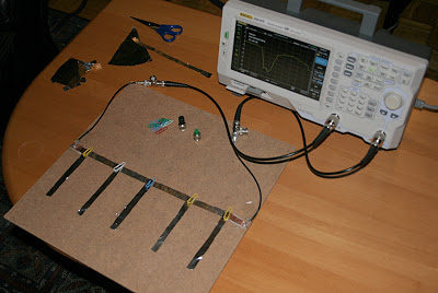 |
| The Microstrip Breadboard ™ |
The Microstrip Breadboard! In the following, I’ll describe what it does and why it is totally awesome.
Construction
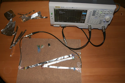
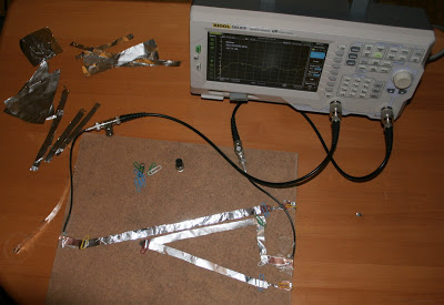
The construction of the board is totally stupid, it’s just two coaxial cables with
BNC plugs screwed to a thin (3mm) wood (or whatever this is?) plate, the
backside of the plate being covered with tinfoil. The cables are mounted with screws, because soldering tinfoil sucks quite badly. The ground leads of the cables are connected to the backside of the board (or rather, the tinfoil there). The top side has two thin copper sheets connected to the signal wires of the cables, which can be used as ports for any structure you build onto the board.
For connecting two tinfoil snipptes, I use (isolated) paper clips. This works pretty well, an alternative solution would possibly be using pins or nails. The main problem with paper clips is that the tracks don’t stay flat on the board, but instead tend to hover a bit, which screws up their impedance. If it gets too bad you can put heavy, non-conductive objects on top of them, or just tape them to the board temporarily.
For measurement, a spectrum analyzer with tracking generator is being used. A vector network analyzer would be optimal for this purpose, but this is just fine too. The analyzer works for frequencies up to 1.5 GHz, and let’s be honest — you don’t want to construct anything from tinfoil and tape for more than 1.5 GHz anyways 😉
The tracking generator output is connected to the left side of the board, and the spectrum analyzer input is connected to the right side. I’ll nickname the left port “1” and the right one “2”, thus “S21” will mean “the part of the signal that went from port 1 to port 2”.
Transmission lines
The width of a 50 Ohm line on my board (3mm thickness, wood) is about 1cm (probably a bit more, but I don’t know the dielectric constant of the wood accurately enough). To calculate that, you can use any program which has a microstrip calculator, such as qucs. You can also calculate it by hand, but why would you?
Here’s what you get when you connect a 30cm length 1cm width line to the two ports of my board:
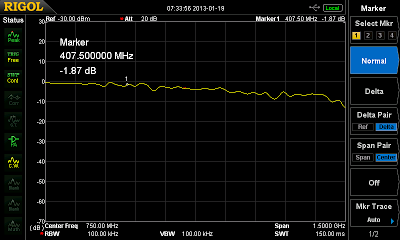 |
| S21 of a 30cm length, 50 Ohms line on the breadboard. |
Obviously there’s some loss, especially at higher frequencies — but seriously, this is tinfoil-tape-RF-land! Considering that, I think the flatness of the curve is great (it’s much better than I expected, anyways).
You can consider calibrating your analyzer to treat this loss as zero loss. I mostly chose not to, but for some structures it might be a good idea.
Building filters
Next, I built some filters. Note that altough I comment on how well those filters perform, this is just describing the experiment, not trying to rank the design ideas or anything. I’m well aware that a tinfoil implementation of the filters is not enough to judge the designs in any way.
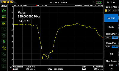
First is the simplest design from the first image (top of the post). It’s just five quarter-wavelength stubs connected to the line. The expected result is a band-stop filter.
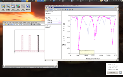
Now you might ask why the curve goes down so much in the end (around 1.5GHz)… well, turns out it’s the second harmonics of the filter, as this simulation shows (in case you find it hard to imagine — if you think about what the standing wave in the stub looks like, it’s pretty clear why this filter also blocks waves which are three times the wavelength given by the stub length):
It’s always nice when physics works.
Next, a bandpass filter made of some parallel lines. The length of the lines is about 12 cm, so the pass frequency should be somewhere around 900 MHz.
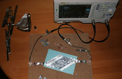 |
| 900MHz Bandpass filter made from some parallel transmission lines. |
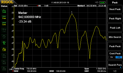 |
| Frequency response of the filter shown above |
Well, this one is pretty crappy, the stopband rejection is just about 12dB lower than the passband value, and even that one is very bad with -23dB. But at least the center frequency matches the calculated one “within production tolerances” 😉
Next, a lowpass filter made from two “inductors” and a “capacitor”:
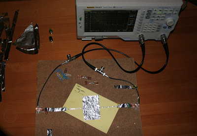 |
| 900 MHz lowpass filter |
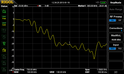 |
| Frequency response of the lowpass filter shown above |
This isn’t too great either, but okay, at least it lets low frequencies pass and rejects high ones. This filter is only first-order, so you probably can’t expect much. Unfortunately this one is pretty large, so I don’t have space for testing how higher orders perform.
Next is another bandpass using a resonant patch between two feed lines:
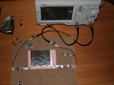 |
| Another bandpass filter designed for 1GHz frequency |
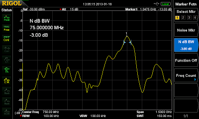 |
| Frequency response of the 1GHz filter shown above |
I like this one very much. It’s pretty easy to build, and with -13dB loss and about -30dB stopband rejection it’s by far the best bandpass filter I taped together. This test thing here is only first order, too, so by putting two of them in a row one could probably improve the result.
And one thing must not be missing, of course… the magic arcs:
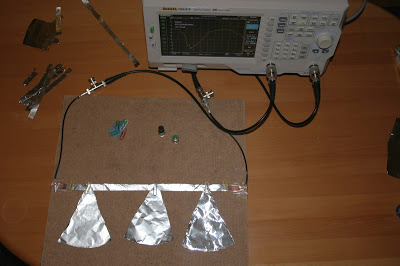 |
| “Magic arc” bandstop filter, with three arcs for a “sharper” response pattern |
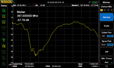 |
| Frequency response for the arc filter |
For these, I don’t really understand how they work… the idea seems to be the same as with the simple stubs, and there’s some extra capacity and inductivity due to the varying width of the arc, but how and why exactly this all fits escapes my mind. For now. Anyways, their filter properties are quite okay, rejection is good and there’s close to no loss in the pass bands, but the bandwidth is huge.
Directional Coupler
Okay, what else could we do with this thing… how about a directional coupler? Here you go:
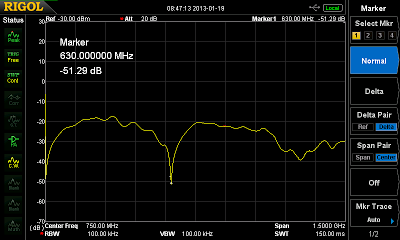 |
| S41 of the coupler, aka what arrives at the coupled port. This plot belongs to the first of the above images. |
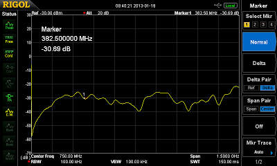 |
| S31 of the coupler, aka what arrives at the isolated port. This one should optimally by -infinity everywhere, but obviously isn’t. This plot belongs to the second of the above images. |
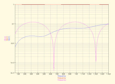
Of couse, I also did a simulation of the coupler by measuring the sizes of the tinfoil pieces with incredible accuracy and typing them into a simulation program:
In my opinion, the match between simulation and measurement is very nice for the S41 curve. For S31 it’s not so obvious, but then again, this value is sort of gibberish anyways. It’s roughly -30dB, that’s enough to know.
It is worth noting that when removing the 50 ohm termination from port 2 (the right one of the upper line in the picture, where the main part of the signal should go out again), then S31 looks quite exactly like S41 (sorry I don’t have a picture). This is correct, since everything is reflected from port 2 and then coupled into port 3.
That’s it for now, if I come across some more microstrip stuff which is nice, I’ll write about it.
Categories: Everything

Considering the cheapness of the materials used, the results are totaly incredible.
Congratulations!
Very instructive! Congratulations!